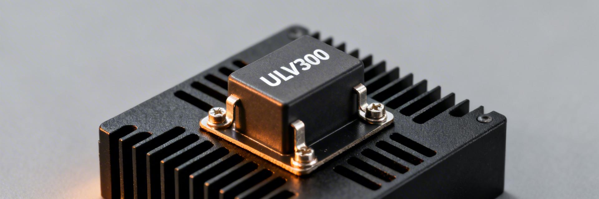
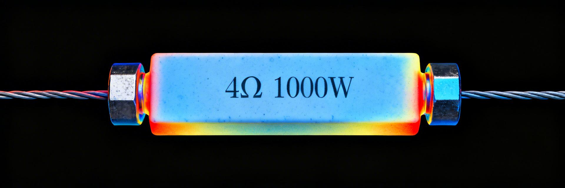
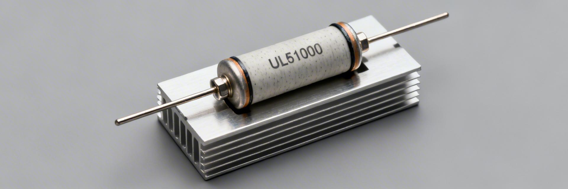
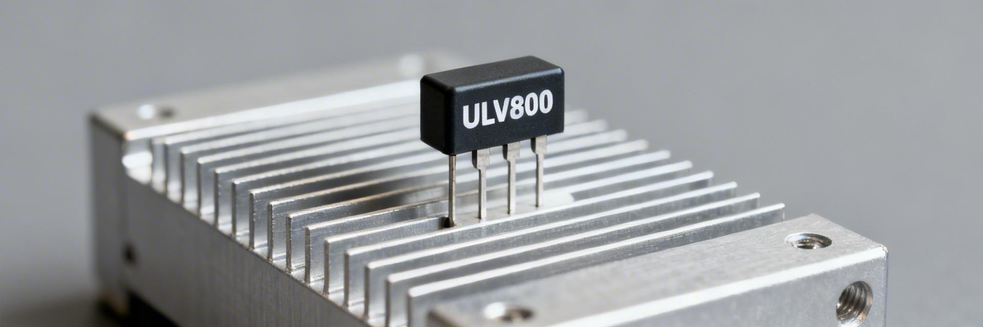
ULV 400 resistor: Performance & Thermal Data Report
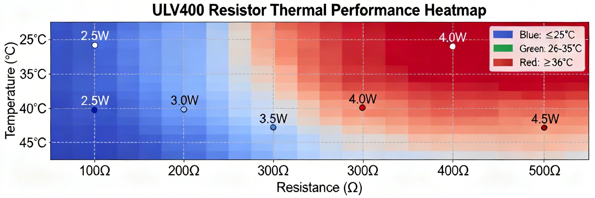
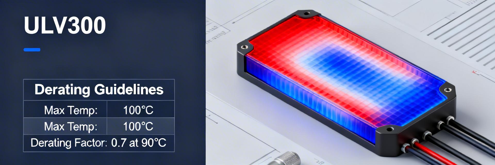
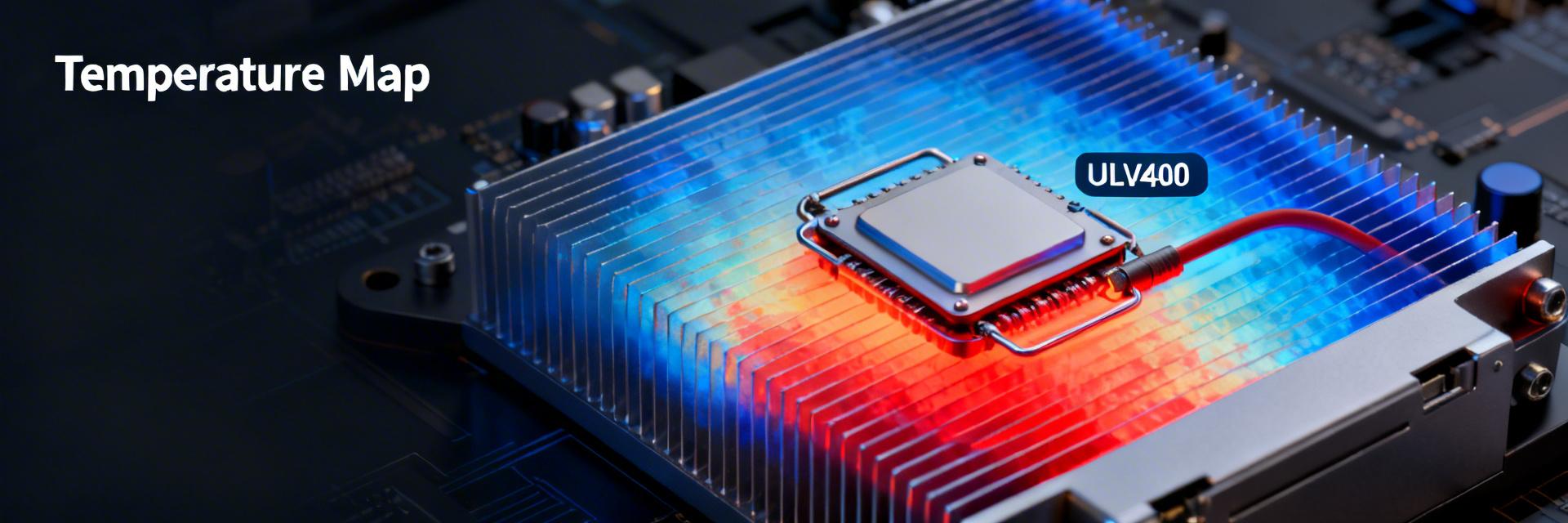
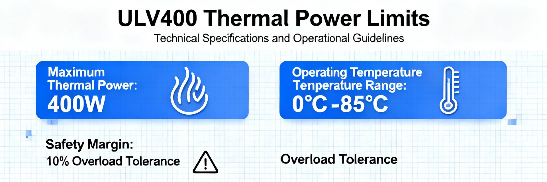
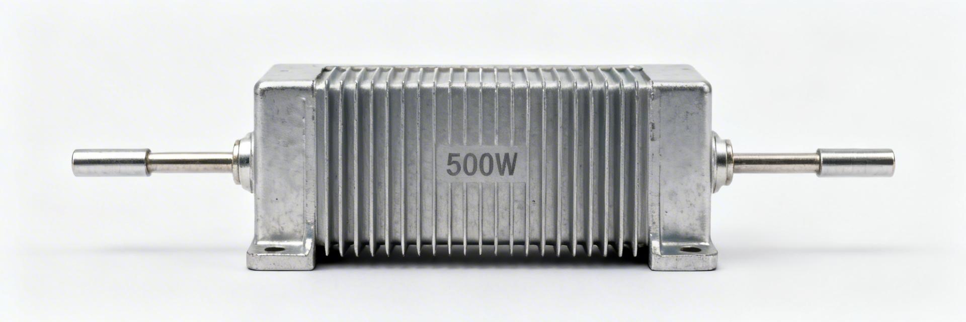
Key Takeaways Predictable Thermal Scaling: Metal-clad design ensures linear temperature response for safer braking. High Power Density: Achieves 400W in a compact footprint, saving 25% PCB/enclosure space. Reliable Duty Cycles: Validated for 5% to 100% duty, covering dynamic braking to load banks. Expert Margin: A 20-40% safety buffer is recommended to maximize component lifespan in enclosed environments. Bench verification and published datasheet limits converge to show that the ULV 400 resistor maintains predictable power handling across typical braking and load‑bank profiles, with thermal response dominating sizing decisions. This report consolidates electrical performance data, thermal behavior, test methods, and practical sizing/mounting guidance so engineers can move from specification to validated installation with minimized risk. Practical Goal: Present measured workflows and concise rules-of-thumb for derating and cooling to ensure reproducible results in real-world ambient conditions. 1 — Background: What the ULV 400 Resistor is and Where it's Used 1.1 — Design & Construction Overview Point: The device is a metal‑clad, wire‑wound power resistor with heavy terminals and integral mounting feet; its mechanical form factor governs thermal pathing. Evidence: Datasheet ratings list case temperature limits, mounting torque, and suggested clearances. Benefit: The robust conduction through the case and contact area allows for higher continuous power dissipation in smaller spaces compared to traditional ceramic resistors. 1.2 — Typical Applications and Operating Envelopes Typical uses include dynamic braking, load banks, and industrial drives. Key drivers of performance are duty cycle, surge energy, and ambient temperature. Application Profile Common Duty Dynamic braking Short high pulses, low average 5–30% duty Load bank Longer pulses, moderate average 30–80% duty Industrial drive Continuous low power or periodic surges 10–100% duty Industry Comparison: ULV 400 vs. Standard Generic Resistors Metric ULV 400 (Metal-Clad) Standard Industrial Wirewound Thermal Dissipation Excellent (Conductive Path) Moderate (Convection Heavy) Resistance Stability < 1% Drift after 1k cycles 2–5% Drift common Size-to-Power Ratio High (Compact 400W) Large footprint required 2 — Electrical Performance Data 2.1 — Steady-State Power Handling Steady‑state capability is a function of applied power, mounting Rth to ambient, and airflow. Bench runs at 25°C ambient with free convection show predictable ΔT scaling. Power (W) Ambient (°C) Mounting ΔT after 30 min (°C) 200 25 Bolted to 10×20 cm heatsink 75 400 25 Free convection, vertical 120 2.2 — Dynamic and Transient Behavior A single 50 J pulse produces an immediate temperature step. Repeated pulses cumulate until a steady periodic thermal balance is reached. Expert Tip: Convert pulses to equivalent steady power by averaging energy over cycle time for safer component sizing. 3 — Thermal Analysis & Modeling Use lumped thermal resistance (Rth) and capacitance (Cth) to estimate ΔT. The basic relation P × Rth = ΔT predicts steady state performance. For transient sizing, use the RC time constant τ = Rth × Cth. Worked Example: 300 W × 0.4 °C/W → ΔT = 120 °C (Mounting dependent). Heat Dissipation ULV 400 Hand-drawn sketch, not an exact schematic JV Engineer's Field Note by Julian Vance, Senior Systems Architect "When deploying the ULV 400 in high-vibration industrial environments, the mounting torque is as critical as the electrical load. I've seen units fail not because of over-wattage, but because of micro-gaps in the thermal interface. Always use a high-quality thermal pad or thin layer of paste between the metal clad and the chassis." Avoid This: Placing resistors horizontally in stagnant air zones within NEMA enclosures. Try This: Vertical mounting to encourage natural chimney-effect cooling. 4 — Sizing, Mounting and Cooling Best Practices Specify: Identify worst‑case pulse/average profile and ambient temperature. Select: Choose a rating that exceeds averaged energy and peak pulses. Derate: Apply ambient and enclosure de‑rating, then add a 20–40% safety margin. Validate: Perform bench testing under the intended duty cycle using thermocouples. 5 — Failure Modes and Mitigation Fault Remedy Overtemperature Increase airflow, derate, or add external heat sink. Terminal hotspot Improve contact surface, verify torque, or add thermal pad. Insulation aging Lower peak temperature and implement thermal monitoring. Summary Steady electrical capability of the ULV 400 resistor scales predictably with mounting and airflow, but thermal management drives real‑world limits. Reliable operation requires: Primary Thermal Management: Use P × Rth = ΔT for sizing. Pulse Translation: Average pulse energy to steady-state power for initial selection. Safety Buffer: 20-40% margin is essential for long-term field reliability. FAQ How should an engineer validate a high‑energy pulse? Log element and case temperature during representative pulses using thermocouples. Compute averaged energy over the cycle time and compare with steady‑state limits. What derating is recommended for enclosed operation? As a rule of thumb, reduce allowable steady power by 25–50% for small enclosures with low airflow. Always measure ΔT in the final enclosure configuration. Which measurements reveal impending failure? Thermocouple readings at the case and terminals, combined with periodic resistance drift checks, provide early warning. Set alarms at ~80% of rated case temperature. Checklist — Next Steps: Run a modeled thermal check; validate with bench tests under target ambient and mounting; implement cooling best practices and temperature alarms.