• MDP16031K00GD04 Datasheet: Full Spec Breakdown & Benchmarks

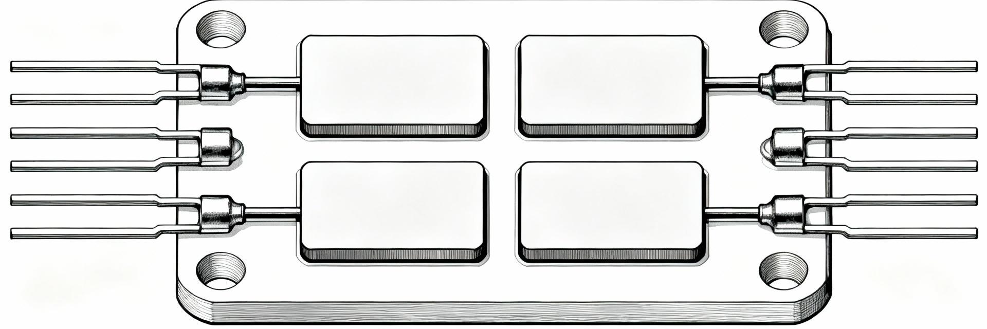
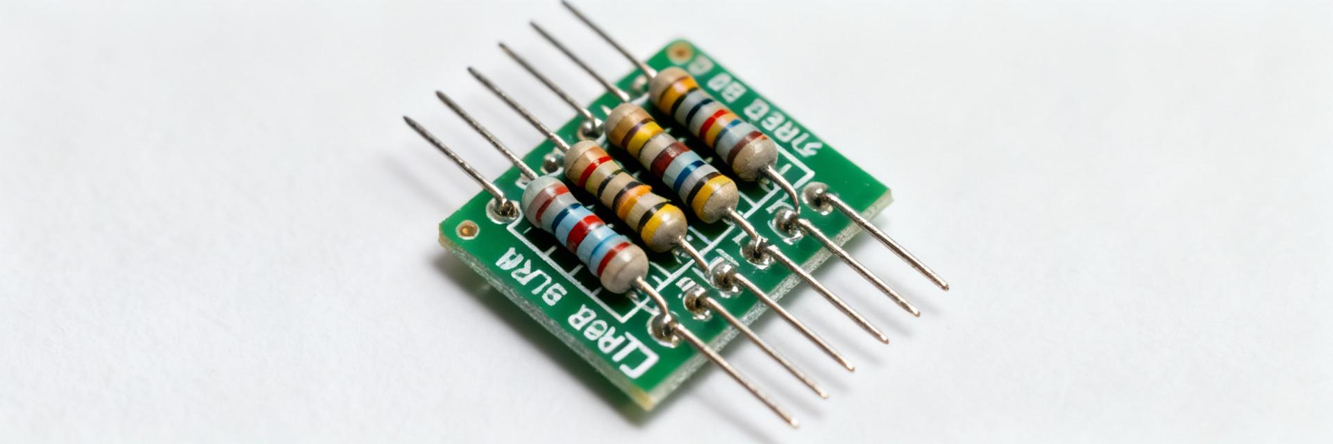
    The MDP16031K00GD04 is a 16‑pin resistor network with a 1 kΩ nominal value, ±2% tolerance, 0.25 W per element and a 100 ppm/°C temperature coefficient — specs that make it a compact choice for matched‑resistance applications. This article provides a datasheet‑driven spec breakdown, reproducible bench benchmarks, practical design implications, and an actionable checklist for engineers. Using measurable test procedures and PCB guidance, the goal is to help engineers validate power derating, matching behavior and board‑level thermal limits before committing to production. The write‑up focuses on repeatable methods, clear pass/fail criteria and concise procurement verifications that integrate with standard qualification workflows. 1 — Background: What MDP16031K00GD04 Is and Where It Fits 1.1 Part family overview & common use cases Point: The device is a through‑hole resistor array (resistor network/array) intended for compact matched networks. Evidence: Typical topologies include isolated arrays and bussed configurations for pull‑ups, sensor divider arrays and trimming. Explanation: Compared with single resistors, networks save board area and improve matching by sharing thermal and process history, simplifying assembly for matched‑pair circuits. 1.2 Key mechanical summary (package & pin count) Point: Mechanical form is a 16‑pin through‑hole package with standard DIP footprint. Evidence: Pin count and lead spacing match common DIP land patterns used for compact arrays; consult the datasheet mechanical drawing for exact dimensions. Explanation: Designers should verify hole diameter and pad annulus against their PCB house rules and plan placement to avoid interference with adjacent components. 2 — Pinout, Package Dimensions & PCB Footprint Guidance 2.1 Pinout and pin functions (how to read the datasheet table) Point: Read the datasheet pinout table to map resistor ends and any common rails. Evidence: Standard numbering lists each element terminals and any shared pins; an annotated pinout figure clarifies which pins form each 1 kΩ element. Explanation: Create a labeled schematic symbol and board‑level silk outline to prevent swap errors during assembly and testing. Figure: recommended annotated pinout (include in design documentation). 2.2 Package mechanicals, recommended footprint, thermal pads Point: Use a conservative land pattern for through‑hole soldering and mechanical integrity. Evidence: Recommend plated‑through holes sized per PCB vendor rules, 0.8–1.0 mm drill for typical leads, and 2.54 mm pitch spacing for DIP rows. Explanation: For reliable solder fillets avoid excessive copper pours directly beneath the part; thermal vias are usually unnecessary but maintain clearance from high‑power traces. 3 — Electrical Specs & Thermal Ratings: Datasheet Deep Dive 3.1 Core electrical specs to call out Point: Core specs determine suitability for matched networks. Evidence: Key rows are nominal resistance 1 kΩ, tolerance ±2%, power per element 0.25 W, tempco 100 ppm/°C, isolation between elements and maximum working voltage. Explanation: Tolerance and tempco directly affect divider accuracy and matched‑pair stability; include these in error budgets for ADC references and sensor dividers. ParameterValue Nominal resistance1 kΩ Tolerance±2% Power per element0.25 W Tempco100 ppm/°C 3.2 Thermal derating, operating temperature range & reliability notes Point: Power handling reduces with temperature; designers must derate. Evidence: If rated 0.25 W at 25°C and linear derating to 0 W at maximum temperature, then at 70°C allowable power may be ~0.15 W. Explanation: Estimate board‑level dissipation using element I²R and account for proximity to copper pours; add a margin for long‑term drift and humidity stress in reliability budgets. 4 — Benchmarks & Test Methodology (data-driven) 4.1 Recommended test setup and measurement procedure Point: Use controlled, repeatable measurements to validate specs. Evidence: Four‑wire resistance measurements avoid lead resistance error; use low test current to avoid self‑heating and perform thermal soak cycles to characterize tempco. Explanation: Include a temperature chamber or heat source and a data‑logger to record time‑stamped resistance vs temperature and time for reproducible trending. 4.2 Representative benchmark results to collect (and how to present them) Point: Collect metrics that reveal real‑world behavior. Evidence: Track initial resistance spread, thermal coefficient validation, board‑level power handling and long‑term drift over accelerated hours. Explanation: Present summary tables for distribution statistics and plots for drift vs time and temperature, then interpret deviations versus datasheet specs to decide accept/reject criteria. Figure: example benchmark plot (include measured data plots in reports). 5 — Comparative Analysis & Application Impact 5.1 How the MDP16031K00GD04 performs versus typical resistor-network options Point: Performance tradeoffs depend on matching and power needs. Evidence: The part offers compact matched elements with modest power per element versus discrete SMD resistors that can provide higher power or tighter tolerances. Explanation: Choose this network when space and matching outweigh higher per‑element power or when assembly simplicity is a priority. 5.2 Real-world implications: signal integrity, sensor interfaces and analog front-ends Point: Tolerance and tempco affect front‑end accuracy. Evidence: A ±2% initial tolerance plus 100 ppm/°C drift can shift divider ratios and ADC reference levels under temperature change. Explanation: Mitigate with calibration, trimming, or placing reference networks in thermally stable regions and adding guard routing for noise‑sensitive traces. 6 — Design, Procurement & Verification Checklist 6.1 PCB and thermal layout checklist Point: Follow concrete layout rules to protect performance. Evidence: Include correct pad sizes, keepouts for solder fillets, trace width to carry element dissipation, test points for in‑circuit verification and avoid routing high‑power traces under sensitive analog nets. Explanation: Use short thermal paths to ground pours only where necessary and maintain distance from heat sources to reduce mismatch from thermal gradients. 6.2 Datasheet validation checklist and procurement notes Point: Validate supplied documentation before procurement. Evidence: Verify part marking, lot code traceability, and request supplier test reports or sample qualification tests. Explanation: Ask for measured lot statistics and any available burn‑in or humidity test data to ensure delivered parts meet the datasheet performance required by your application. Key summary MDP16031K00GD04 provides 1 kΩ, ±2% matched elements with 0.25 W per element — suitable for compact matched networks and divider arrays. Thermal derating and layout matter: derate power at elevated ambient, avoid large copper under the part, and add thermal margin on sensitive paths. Bench tests should include four‑wire resistance, thermal soak cycles and long‑term drift plots to validate datasheet specs before production. Frequently Asked Questions What are the key specs I should verify on the datasheet? Verify nominal resistance, tolerance, power per element, temperature coefficient and maximum working voltage. Also confirm mechanical drawings for hole size and pitch, and request supplier test reports for lot‑level variation to align procurement with design margins. How should I test for thermal derating on the PCB? Use a controlled chamber to measure resistance and power dissipation at multiple ambient temperatures. Apply the expected board current to an element, log temperature and resistance over soak intervals, and compare measured dissipation limits to the datasheet derating curve for pass/fail decisions. When is a resistor network better than discrete resistors? Choose a network when matching and compactness are priorities and per‑element power needs are within specified limits. Discrete resistors are preferable when higher power, tighter tolerance, or layout flexibility outweigh the benefits of integrated matching. Conclusion (summary & key takeaways) The MDP16031K00GD04 offers 1 kΩ elements with ±2% tolerance, 0.25 W per element and 100 ppm/°C tempco, making it a good fit for compact matched networks and divider arrays where space and matching matter. Key considerations are power derating, PCB layout and verifying matched tolerance in your application. Use the checklist above to validate the part against your board‑level thermal and accuracy requirements before committing to production.
  • TDP16035002AUF Datasheet: Precision Specs & Metrics

    The following data-driven summary highlights the precision metrics that matter most to analog designers: number of resistors, package type, typical tolerance, channel-to-channel matching, temperature coefficient, ratio drift, and operating temperature range. These metrics determine gain error, offset drift, and long-term stability in precision instrumentation and ADC front-ends. This introduction sets expectations for interpreting a datasheet and planning verification and integration steps using clear electrical and mechanical criteria. Key terms used in this article include datasheet and precision specs, with focused coverage on resistor network characteristics, thin-film resistor behavior, and resistor array considerations relevant to precision analog designs in the US market. At-a-glance technical overview — TDP16035002AUF key specs (background) Quick technical summary (one-table snapshot) The table below presents a compact specification snapshot to use as a hero reference when evaluating the part for board-level designs. Confirm exact test conditions in the official datasheet before design-in. Spec at a glance ParameterValue (typ / max) Part typePrecision thin-film resistor network Number of resistors4 elements Nominal resistances10 kΩ, 100 kΩ options Tolerance±0.1% typ / ±0.5% max Channel-to-channel matching±0.02% typ / ±0.05% max Ratio drift≤ 2 ppm/°C typ Temperature coefficient (TCR)5 ppm/°C typ Package8-pin SMD, gull-wing Operating temp range-55°C to +125°C Power rating per element125 mW at 70°C derated Intended applications and product fit Resistor networks like this target precision instrumentation, sensor front-ends, ADC input networks, and bridge circuits. Tight resistor matching reduces differential gain error, low TCR limits temperature-induced offset, and small ratio drift preserves calibration over environmental swings. Use cases include low-noise instrumentation amplifiers, high-resolution ADC inputs, and low-drift Wheatstone bridges where cumulative mismatch drives measurement error. Electrical characteristics & precision metrics from the datasheet (data analysis) Resistance values, tolerance, and channel-to-channel matching Nominal resistance options are typically offered in standard E24/E96 values; tolerance and channel matching are separate specs. Typical tolerance may be ±0.1% with worst-case ±0.5%. Channel-to-channel matching of ±0.02% typical (±0.05% max) governs differential error. Test conditions are usually 25°C and a specified measurement current—confirm these before acceptance testing. Example calculation: a differential amplifier with resistor pair matched at ±0.05% yields a gain error ≈ 0.0005 (0.05%). For a nominal gain of 100, that mismatch causes ~0.05 gain error, directly impacting LSB accuracy on a 24-bit ADC. Design margin should allocate additional budget for tolerance, drift, and measurement uncertainty. Temperature coefficient, stability, and long‑term drift TCR given in ppm/°C converts to relative resistance change: ΔR/R = TCR × ΔT. For 5 ppm/°C over a 100°C swing, change is 500 ppm (0.05%). Ratio drift often specified separately (e.g., 2 ppm/°C) and is the critical figure for matched elements. Long-term drift may be stated in ppm/year—plan for worst-case cumulative change over product lifetime and include calibration intervals if needed. Worst-case drift across operating range SpecΔR/R over -55°C→125°C TCR 5 ppm/°C~0.4% (4000 ppm) Ratio drift 2 ppm/°C~0.16% (1600 ppm) Mechanical, packaging, and thermal limits (data analysis) Package, pinout, and footprint guidance Package is an 8-pin SMD with standard gull-wing leads. Confirm exact outline dimension block for pad land pattern. Recommended PCB footprint uses solder fillets sized to manufacturer-recommended land pads; maintain equal trace lengths for matched resistors and provide thermal symmetry. Keepout zones under the package reduce thermal conduction differences between elements. Power rating, derating, and thermal performance Per-element power rating commonly 125 mW at 70°C, derated to zero at maximum temperature. Use a linear derating curve: full power at 70°C, 50% at 100°C, zero at 175°C as a conservative example. Thermal resistance and ambient mounting affect self‑heating; rule of thumb: limit continuous dissipation to 50% of rated power for high-precision circuits to avoid thermally induced matching shifts. How to read, interpret, and verify datasheet numbers (method guide) Interpreting “typical” vs “maximum” and test-condition callouts “Typical” indicates median or common performance; “maximum” is guaranteed under specified test conditions. Always check the test temperature, applied current, and measurement method. Red flags include unspecified test conditions, ambiguous units, or missing ratio-drift spec. Checklist: note test temp, measurement current, sample size, and qualification method before design-in. Recommended bench verification protocol for precision specs Verification equipment: precision DMM (0.1 ppm resolution desirable), stable current source, temperature chamber or hotplate. Steps: measure tolerance at 25°C, measure channel-to-channel matching under identical excitation, run temperature sweep to derive TCR and ratio drift, and record long-term stability if possible. Suggested sample size: 10 units per lot with statistical checks (mean, sigma). Pass/fail thresholds should be set tighter than datasheet max to allow margin for system error. Case study — bench comparison and integration metrics (case) Example bench test results & data visualization Hypothetical results: measured tolerance mean ±0.09% (spec ±0.1%), matching mean ±0.018% with 3σ = 0.04% (spec max ±0.05%). A histogram of channel-to-channel variation and resistance-vs-temperature plots expose outliers and slope. Replicate graphs: histogram of ΔR/R, resistance vs temperature line fits, and a derating curve overlay to visualize safe operating regions. When channel-to-channel matching or ratio drift dictates design choices Scenario A: high-resolution ADC front-end—prioritize matching and low ratio drift to limit gain error; choose networks with ≤0.02% matching. Scenario B: Wheatstone bridge—matching dominates offset; prefer networks with low ratio drift and thermal symmetry. Quantify impact by converting ppm drift into equivalent voltage offset at expected bridge excitation. Selection checklist & integration tips for engineers (action) Pre‑selection & procurement checklist Before ordering: confirm exact resistance option, tolerance and matching specs, package and pinout, operating temperature range, per-element power rating, and availability/supply considerations. Order samples across production lots to evaluate lot-to-lot variation; request characterization data from the vendor if available. Verify part marking and MOQ to align with QA sampling plans. PCB layout, de‑rating, and assembly tips for preserving precision Layout tips: route matched traces symmetrically and keep lengths equal; avoid routing high-power traces adjacent to resistor arrays; place thermally active components away from the network. For SMD parts, follow recommended reflow profiles and post-reflow cleaning that avoids flux residue under packages. Include test pads for in-circuit trimming or calibration and reserve space for shunt resistors if needed for calibration. Summary Nominal resistances and tolerance: choose the value that minimizes excitation current while keeping tolerance and matching within system error budget; tight tolerances reduce initial calibration needs. Channel-to-channel matching and ratio drift: these determine differential gain and temperature-induced offset; prioritize low ppm/°C ratio drift for precision ADCs and bridges. Thermal and power considerations: derate per-element power conservatively, maintain thermal symmetry on the PCB, and limit self-heating to preserve matching and long-term stability. Verification and procurement: run a bench protocol with a precision DMM and temperature sweep, sample multiple lots, and require vendor test conditions before full production sign-off. Integration tips: use symmetrical routing, test pads for calibration, and conservative derating rules to maintain long-term precision. Final note: consult the TDP16035002AUF datasheet — precision specs as the authoritative source for guaranteed limits and test conditions when finalizing component selection and validation plans. Frequently Asked Questions How does the TDP16035002AUF matching specification affect ADC front-end accuracy? Channel-to-channel matching directly determines differential gain error in ADC front-ends. A ±0.05% matching limit can introduce proportional gain error; lower matching (±0.02% or better) reduces this source of error. Designers should budget matching error into total system error and consider calibration if necessary. What test conditions are recommended to verify the datasheet tolerance and temperature coefficient? Verify tolerance at 25°C with a stable current source and precision DMM. For TCR, perform a controlled temperature sweep (e.g., -55°C to +125°C) in a chamber and record resistance at multiple points to fit ppm/°C. Ensure measurement uncertainty is smaller than the spec you intend to verify. When should I prioritize resistor array matching over nominal tolerance in selection? Prioritize matching when differential accuracy or ratio stability drives system performance—examples include instrumentation amplifiers and bridge sensors. If the application is single-ended or can be recalibrated frequently, nominal tolerance may be sufficient; otherwise, choose networks with tighter matching and lower ratio drift.
  • MPM10011002AT0 datasheet: SOT-23 divider specs & tests

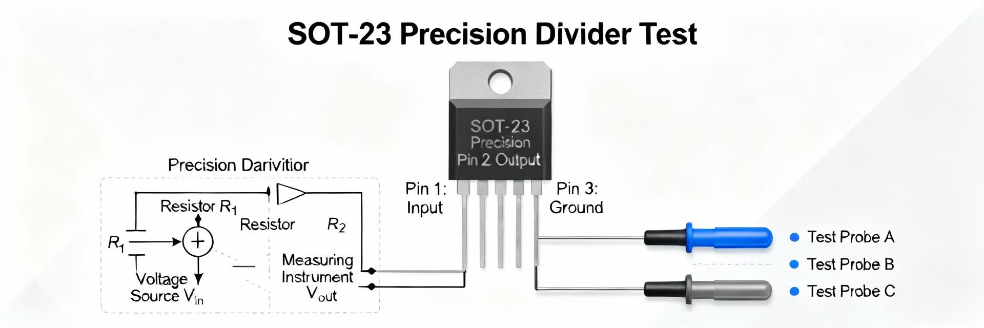
    Compact matched resistor dividers such as the MPM10011002AT0 play a precision role in small-footprint voltage references and gain-setting networks. Typical design drivers are tight ratio tolerance (single-digit ppm tracking), low tempco tracking, milliwatt-class power per element, and limited max working voltage. This article targets hardware engineers and test technicians and explains how to read the MPM10011002AT0 datasheet, verify SOT-23 divider specs, and run repeatable bench tests. The goal is practical: extract the critical numbers from the official datasheet, translate them into pass/fail criteria, and document tests for reproducible validation. The text refers to the official datasheet for every quoted numeric spec (annotated as "official datasheet"). It shows required bench setups, measurement steps, and expected plots so engineers can validate parts before committing them into precision analog designs. Background: What the MPM10011002AT0 is and SOT-23 divider overview Key specs at a glance (author: build a 1-row summary table) Field Value (official datasheet) Nominal resistances See official datasheet (copy exact R values here) Ratio and ratio tolerance See official datasheet (annotate ratio tolerance, e.g., ppm or %) Individual resistor tolerance See official datasheet (e.g., ±0.1% etc.) Power per element (mW) See official datasheet Max working voltage (V) See official datasheet Temperature coefficient (ppm/°C) See official datasheet Package SOT-23 (3-pin) — official datasheet Operating temperature range See official datasheet Note: copy the numbers verbatim from the official datasheet into the table above and flag model variants where the datasheet lists alternate tolerances or resistance codes. This table is the single-row "at-a-glance" summary for quick engineering decisions. The SOT-23 divider specs shown in the table let designers balance footprint vs performance. Typical applications and why SOT-23 dividers matter Matched divider networks in SOT-23 packages are chosen for precision voltage references, ADC front-end scaling, and gain-setting where matching and thermal tracking are more important than absolute resistance. Compared to discrete resistors, integrated networks reduce mismatch and thermal gradients at the expense of per-element power capability and maximum working voltage. Use them when space and tracking are critical and when expected power dissipation stays within the part's per-element mW rating. Electrical specifications deep-dive (data analysis) Ratio tolerance, tracking, and matching: what to look for in the datasheet Distinguish ratio tolerance (relative error between resistor elements) from absolute tolerance (each resistor vs nominal). Ratio tolerance controls divider output error directly; absolute tolerance affects absolute resistance but not the ratio as strongly. Read the datasheet fields labeled "ratio" or "divider tolerance" and "element tolerance" and annotate the units (ppm or %). For example, convert a ratio tolerance of X ppm to expected output error by: error (%) ≈ X × 1e-4. When reporting, always annotate "official datasheet" next to quoted numbers. Tracking tempco (ppm/°C differential between elements) is critical for stability over temperature. If tracking is T ppm/°C, a 50°C swing produces ≈50·T ppm ratio drift. Use that to budget worst-case divider drift in the system error budget. Power, voltage coefficient, and temperature limits Power per element (mW) indicates safe DC current for each resistor. Use P = V^2/R_element to estimate self-heating and compare to per-element rating from the official datasheet. Voltage coefficient (ppm/V) quantifies ratio change with applied voltage; if the datasheet lists VC = Vc ppm/V, then Δratio_ppm ≈ Vc × ΔV. Read the maximum working voltage and test voltages on the official datasheet and apply conservative derating (see Design & application recommendations) when designing precision references. Test setup & measurement procedures (method guide) Recommended bench setup and instruments Required tools: calibrated 6½-digit DMM or resistance bridge for ratio and resistance, low-noise DC source able to drive required V and current, temperature chamber or hotplate for tempco, Kelvin fixtures and microscope for handling SOT-23. Use a 4-wire method for resistance/ratio wherever possible. Account for measurement uncertainty by budgeting instrument accuracy, lead resistance, and thermal EMF; document calibration steps before tests. Step-by-step test procedures to include DC resistance and ratio: measure N≥10 samples per lot. Use 4-wire Kelvin connections; record R1, R2, and computed ratio R1/(R1+R2). Log unit IDs and ambient. Temperature coefficient: place samples in chamber; step in 10–20°C increments, allow stabilization (10–30 min depending on chamber), measure ratio at each point and plot Δratio vs T. Voltage coefficient and power-induced drift: apply nominal Vin and step to the datasheet max working voltage (and one above for margin), measure ratio shift vs applied V. Long-term stability: accelerated aging or thermal cycling (e.g., 100 cycles -40°C to +85°C) can highlight solder/reflow issues. Expected outputs: ratio error in ppm, absolute resistance drift in ppm, plot formats and pass/fail compared to official datasheet limits. Example bench results & interpretation (case study) Example result sets to present and how to visualize Present: (1) ratio error histogram (ppm), (2) ratio vs temperature plot (ppm vs °C), (3) ratio vs applied voltage (ppm vs V). Good parts cluster within the datasheet ratio tolerance; outliers beyond tolerance should be flagged. Use axis labels: "Ratio error (ppm)", "Temperature (°C)", "Applied voltage (V)". Annotate pass/fail thresholds from the official datasheet on plots for clarity. Common deviations, root-cause analysis, and troubleshooting Common sources of discrepancy: measurement error (poor 4-wire connections, thermal EMFs), self-heating from test current, solder damage from reflow, and package stress. Corrective steps: switch to 4-wire measurement, reduce test current, improve thermal anchoring, reflow with recommended profile, and inspect solder fillets under microscope. Re-run tests after corrective actions and compare to initial baseline. Design & application recommendations (action checklist) PCB layout, thermal management, and derating Keep divider networks away from localized heat sources; use copper pours to stabilize thermal gradients. Place thermal vias under adjacent areas if heat spreading is needed. For SOT-23, follow recommended solder profile to avoid stress. Derate voltage and power: operate at ≤60–75% of the datasheet max working voltage/power for precision applications to reduce self-heating and VC effects. Selecting equivalents and specification trade-offs When comparing alternate SOT-23 dividers, prioritize ratio tolerance, tracking tempco, and voltage coefficient. Prefer discrete resistors when per-element power or working voltage exceeds the integrated network limits. Procurement checklist: required ratio tolerance, operating temperature, per-element power, voltage coefficient, and package compatibility. Summary This guide shows how to extract and validate the critical fields in the MPM10011002AT0 datasheet, test SOT-23 divider specs on the bench, and interpret results versus official limits. Engineers should quote the official datasheet numbers in reports, use 4‑wire methods, and apply conservative derating to ensure in-system precision. Use the outlined procedures for reproducible, defensible validation of part performance in precision designs. Extract ratio, element tolerance, tempco, and max working voltage directly from the official datasheet and record them as test pass/fail thresholds. Measure ratio with 4‑wire methods and plot ratio error (ppm) vs temperature and applied voltage to reveal tracking and VC issues. Derate to ≤75% of max power/voltage for precision applications to reduce self-heating and voltage-coefficient drift. When out-of-spec, isolate causes: measurement method, self-heating, reflow damage, or package stress, then retest after corrective action. FAQ How to find the exact nominal resistances in the MPM10011002AT0 datasheet? Open the official datasheet and locate the ordering code table or electrical characteristics section; the nominal resistances are listed alongside the part number and tolerance. Always copy the numeric values verbatim and annotate them as "official datasheet" in your validation reports for traceability. What is the best method to measure ratio accuracy for a SOT-23 divider? Use a calibrated 4‑wire resistance bridge or a 6½-digit DMM with Kelvin fixturing to measure each element and compute the ratio. Use low test currents to minimize self-heating, and average multiple measurements after thermal stabilization for best accuracy. How should I account for temperature effects from the datasheet in system error budget? Use the tracking tempco (ppm/°C) from the official datasheet: multiply the tracking tempco by the expected worst-case ΔT to get ppm ratio drift, convert to volts at your Vin to include in the system error budget, and add margin for manufacturing spread and VC effects.
  • NOMC16031003FT5 Resistor Network: Full Spec & Test Data

    At a glance: resistance range and network configuration, tolerance class, per‑element power, package type, and why verifying the NOMC16031003FT5 matters for system reliability. Point: engineers need these baseline numbers to budget accuracy and thermal headroom. Evidence: the datasheet lists nominal values and ratings. Explanation: this note presents spec breakdown, measured test data, and repeatable verification procedures. Goal: provide a concise, repeatable validation plan so an engineer can confirm fit‑for‑purpose before PCB sign‑off. Point: the focus is on reproducible measurements and practical pass/fail thresholds. Evidence: common failure modes impact system gain and offset. Explanation: follow the test plans and PCB guidance below to reduce field risk and design iterations. 1 — Device overview & part-identification (background) Part numbering, package and pinout — explain how to interpret the NOMC16031003FT5 part code, list package options, pinout diagram and footprints to check against PCB land pattern. Content direction: include a simple labeled diagram, recommended footprint checks, and note common misreads when sourcing. Point: decode the part code to confirm the correct resistor network variant for the design. Evidence: part codes encode element count, configuration, tolerance and package. Explanation: verify package pitch and pinout against PCB footprint; confirm the network type and tolerance before placing orders to avoid mistaking similar codes from different families. Simple labeled pinout (text diagram): _________ | 1 . . 8 | | . NOMC | | 8 . . 1 | --------- Key: pins 1–8 correspond to element termini; check datasheet pin map and recommended land pattern. Key electrical features at a glance (spec summary) — provide a concise spec table to be filled from the datasheet: resistance values per element, network configuration (series/parallel/common node), tolerance, TCR (ppm/°C), max working voltage, element power rating, insulation/isolation, and operating temperature range. Content direction: advise authors to annotate each spec with the expected measurement unit and acceptable tolerance. Point: capture critical specs in a single table for bench planning. Evidence: nominal resistance, tolerance, TCR, power and voltage limits determine measurement methods. Explanation: annotate units (Ω, %, ppm/°C, W, V, °C) and acceptable test tolerances when recording results. SpecValueUnit / Note Resistance per element3.01k (example)Ω — verify against datasheet Network config3 resistors, common node— confirm pinmap Tolerance±0.1% TCR±25ppm/°C Power per element0.063W Max working voltage50V Operating range-55 to +125°C 2 — Full electrical specification breakdown (data analysis) Resistance, tolerance and temperature coefficient (TCR) — explain what each spec means for circuit behavior, how tolerance and TCR combine to affect accuracy across temperature, and long-tail keyword suggestions to use in this section (e.g., "NOMC16031003FT5 resistor network spec", "resistor network TCR spec"). Content direction: recommend including formulae for worst-case tolerance stack-up and an example calculation. Point: tolerance and TCR set initial and temperature‑dependent error budgets. Evidence: worst‑case tolerance stack = tolerance + (ΔT × TCR/10⁶ × 100%). Explanation: for a ±0.1% part with 25 ppm/°C TCR and a 80°C swing, temperature contribution = 0.20% so total worst‑case = 0.30%; use this in system accuracy budgeting. Power, voltage and isolation constraints — detail per-element power dissipation, derating rules, maximum working/withstand voltages, and isolation between elements. Content direction: include thermal considerations (ambient vs. PCB thermal resistance) and a small derating table for common operating conditions. Point: element power rating must be derated by board thermal environment. Evidence: package thermal resistance and copper area change allowable dissipation. Explanation: apply derating; if 0.063 W rating at 25°C rises with ambient, reduce continuous power by specified percentage per datasheet guidance and monitor temperature rise in thermal simulations. AmbientDerating factor 25°C100% 60°C70–80% 85°C≤60% 3 — Test data: measured results & typical performance (data analysis) Test setup and measurement conditions — specify repeatable lab conditions: sample size, temperature chamber setpoints, instruments (four‑wire source‑measure, LCR meter, micro‑ohm meter), test-fixture guidelines, measurement cadence, and logging format. Content direction: include a reproducible test plan checklist (ambient temp, soak time, measurement sequence). Point: a repeatable setup reduces measurement variability. Evidence: use four‑wire Kelvin measurement, stable source, and temperature chamber. Explanation: recommended sample N≥30, soak 15 min at temperature, sequence: DC resistance (room), TCR sweep, power soak, isolation test; log CSV fields: ID, temp, measurement, timestamp, operator. Sample size: 30 units minimum. Instruments: 4‑wire SMU, LCR for AC checks, micro‑ohm for Chamber setpoints: -40, 25, 85°C with 15‑min soak. Fixture: gold‑plated Kelvin contacts, minimized lead length. Logging: CSV with metadata and pass/fail flags. Typical measurement results and interpretation — show how to present measured resistance distributions, TCR curves, power-cycle behavior, and isolation/leakage figures (placeholders for actual tables/plots). Content direction: instruct authors to include sample mean, standard deviation, histogram of resistance spread, and pass/fail criteria aligned to the datasheet spec. Point: present statistics, not just individual values. Evidence: include mean, σ, min/max and histogram. Explanation: define pass if |measured − nominal| ≤ tolerance and TCR trend within spec; report percentage out of spec and recommended lot rejection criteria (e.g., >2% units out of spec triggers investigation). 4 — How to verify NOMC16031003FT5: step-by-step procedures (method / actionable) Bench tests for electrical validation — give stepwise procedures for DC resistance, TCR (swept temperature), power dissipation test, and insulation/leakage tests. Content direction: include required equipment settings, contact methods (Kelvin), safety notes, and acceptance thresholds. Point: follow explicit steps to validate electrical performance. Evidence: DC resistance use 4‑wire, TCR sweep in chamber, power test with controlled current ramp. Explanation: example DC test: 1 mA current source, 4‑wire, 10 readings averaged; TCR: measure at −40/25/85°C and compute ppm/°C; power soak: apply rated power for 1 hour and re‑measure resistance shift threshold ≤0.1%. Reliability and stress testing recommendations — outline accelerated tests to expose failures: thermal cycling, power humidity bias, and surge/transient tests relevant to resistor networks. Content direction: list test durations, conditions, what to monitor (resistance shift, open elements), and suggested reporting format. Point: accelerated stress tests reveal marginal parts. Evidence: thermal cycle 500 cycles −40/+125°C, HAST with bias for humidity susceptibility, and surge per expected field transients. Explanation: monitor for open circuits, >1% resistance drift, or insulation breakdown; report per unit: pre/post resistance, percent shift, and condition that triggered failure. 5 — Application guidance, PCB integration & troubleshooting (case/action) PCB layout, thermal management and derating checklist — practical layout tips: placement, copper pour for thermal relief, decoupling, and derating rules for multi-element dissipation. Content direction: provide a short PCB checklist and example scenarios where mis-layout causes derating issues. Point: PCB layout materially affects derating and accuracy. Evidence: copper pours alter thermal resistance and can double allowed dissipation in some cases. Explanation: checklist: verify footprint pad sizes, add thermal vias under high‑dissipation nets, avoid routing narrow traces under network, and allocate derating margin when multiple elements dissipate simultaneously. Common failure modes and troubleshooting flowchart — identify typical problems (open elements, drift, imbalance), root-cause indicators, and stepwise troubleshooting actions (re-measure, thermal imaging, swap with known-good). Content direction: include recommended corrective actions and when to reject a lot based on measured data. Point: identify quick root causes and remediation. Evidence: common signs—open = infinite resistance, drift = temp/time correlated change, imbalance = mismatch between elements. Explanation: troubleshooting: re‑measure with Kelvin, apply gentle power to observe heating, inspect solder joints, replace suspect units; reject lot if >2% units show drift beyond spec. Summary Verify the NOMC16031003FT5 against its datasheet and the provided test plans to confirm nominal resistance, TCR, and power handling before PCB sign‑off; document mean and σ for lot acceptance. Use the included bench procedures and stress tests to expose marginal units; apply derating and PCB thermal controls to maintain long‑term stability and prevent drift. Record structured test data (CSV) with ID, temp, measurement and pass/fail flags so system tolerance budgeting can accept or reject a lot based on quantitative criteria. Frequently Asked Questions What key measurements should be in NOMC16031003FT5 test data? Measure DC resistance (4‑wire) at room temp, TCR across defined temperature points, power‑soak resistance shift, and inter‑element insulation/leakage. Capture sample mean, standard deviation and percent out‑of‑spec. Include measurement conditions and fixture details in the CSV for traceability. How should an engineer measure resistor network TCR reliably? Use a temperature chamber with a stable soak (≥15 min) at each setpoint and a four‑wire measurement. Compute ppm/°C from slope between two temperatures: TCR = (ΔR/R)/ΔT × 10⁶. Repeat on multiple samples and report mean and σ to assess lot variation. When is a lot of resistor networks rejected based on test data? Suggest rejecting a lot if >2% of sampled units exceed datasheet tolerance after conditioning, or if mean shift after power‑soak or thermal cycling exceeds the designed system margin. Document failure modes and perform root‑cause before rework or alternate sourcing.
  • MPMT1002AT5 Datasheet Deep-Dive: Key Specs & Metrics

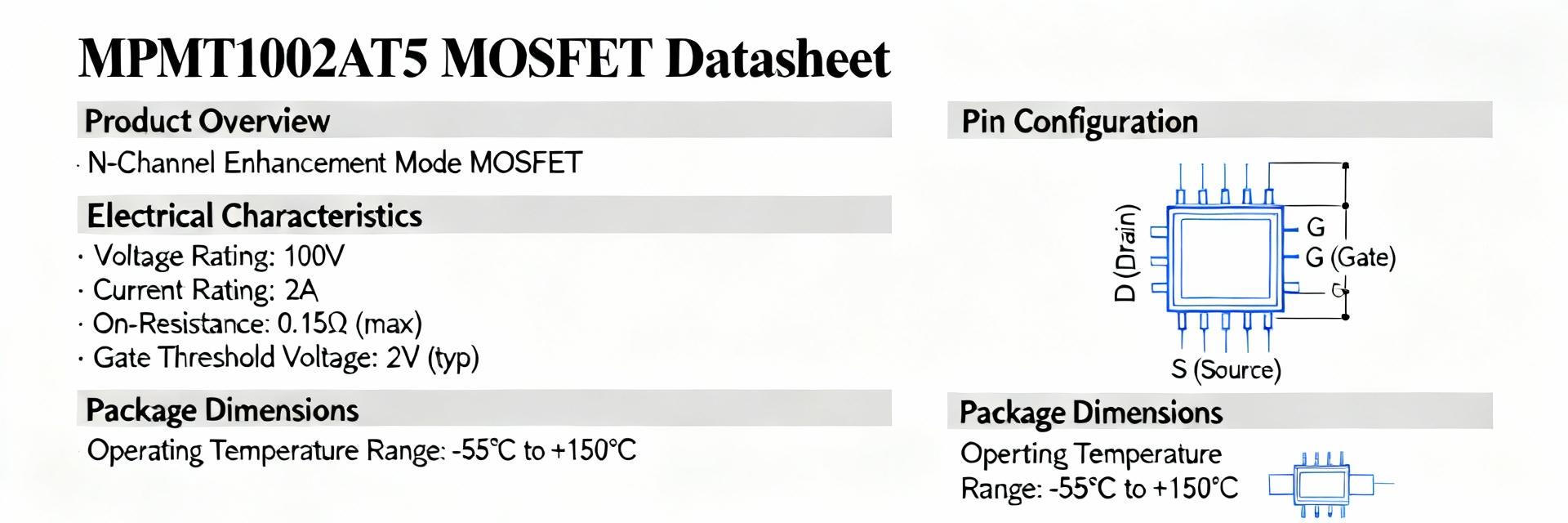
    The latest datasheet contains dozens of electrical and thermal entries; eight typically determine whether a MOSFET meets system-level targets for efficiency, thermal margin, and EMI. This deep-dive extracts the critical specs, explains how to validate them in the lab, and provides practical metrics and trade-offs for topology selection. Readers will see the term MPMT1002AT5 in part-marking and header fields and learn to interpret datasheet numbers and translate them into design decisions. This guide is aimed at power-design engineers, component engineers, and test engineers who need reproducible procedures to validate static and dynamic specs. It covers which fields to read first on the datasheet, methods to estimate conduction and switching losses, thermal impedance interpretation, and a checklist to use before prototype build. The word "datasheet" and "specs" are used throughout to align expectations with measured results. 1 — Background: MPMT1002AT5 at a glance 1.1 Key identifiers on the datasheet Point: Start by locating the part-number block, package code, marking, revision/date and ordering codes. Evidence: The header typically lists part variants and revision identifiers alongside package outlines. Explanation: Confirm the exact MPMT1002AT5 variant and revision: package code indicates thermal pad and leadframe options, marking correlates to internal binning, and revision/date flags spec updates that affect RDS(on) or thermal tables. 1.2 Target applications and typical topologies Point: Identify common use cases such as synchronous buck, synchronous boost and point-of-load converters. Evidence: Device power class, VDS rating, and package thermal performance drive suitability. Explanation: Use a rule-of-thumb: select this device for mid-power point-of-load or buck stages where the package thermal pad and RθJA support the application power dissipation at your switching frequency; match switching frequency to device gate-charge and loss profile. 2 — DC specs deep-dive: static electrical characteristics 2.1 On-resistance, threshold, and leakage Point: RDS(on), VGS(th) and leakage currents define conduction performance and standby budgets. Evidence: Datasheet lists typical and maximum RDS(on) at reference temperature and sometimes at elevated Tj, plus VGS(th) spec and leakage vs. temperature. Explanation: Convert datasheet values to system loss with loss = I^2 * RDS(on) for conduction. Account for temp dependence by using RDS(on) derating from the curve; include worst-case leakage in standby power budgets and for boot-strap or bias supply design. 2.2 Thermal ratings and SOA considerations Point: Extract RθJA, RθJC, Tj(max) and any thermal impedance curves. Evidence: Thermal tables and graphs show how junction temperature rises with power and how RθJA varies with PCB copper area. Explanation: Map thermal impedance curves to your PCB by matching copper area and layer count to the plotted RθJA points. Read Safe Operating Area if present and derate current or duty cycle where the SOA or Tj limit would otherwise be exceeded; prepare a short checklist of thermal fields to capture. Thermal ParameterWhy it matters RθJA / RθJCMaps device power to junction rise and informs copper area needed Tj(max)Defines allowable dissipation for reliability and margin Thermal impedance curvesEnable transient power handling and pulse-width planning 3 — Dynamic specs & switching metrics 3.1 Gate charge, capacitances, and switching times Point: Qg, Qgs, Qgd and capacitances (Coss, Crss) determine driver sizing, switching loss, and dV/dt behavior. Evidence: Datasheet curves provide gate-charge vs. VGS and capacitance vs. VDS. Explanation: Use these specs to estimate gate-driver power (Pdriver = Qg * Vdrive * fSW) and to size the driver for targeted rise/fall times. Map datasheet test conditions (VDS, ID, VGS) to your circuit operating points to ensure comparable interpretation. 3.2 Loss estimation and example methodology Point: Combine conduction and switching contributions to estimate total device loss. Evidence: Required inputs include RDS(on) at operating Tj, Qg, switching frequency and observed dV/dt. Explanation: Step method — 1) calculate conduction loss using I^2·RDS(on) averaged over waveform; 2) estimate switching loss from energy per transition (use published curves or approximate with E = 0.5·Coss·VDS^2 for capacitive contribution plus gate-charge-related switching); 3) add driver losses and margin (suggest 20–40% margin or specify thermal headroom in °C). Document assumptions for repeatability. 4 — How to validate MPMT1002AT5 datasheet numbers in the lab 4.1 Recommended test setups & conditions Point: Reproduce datasheet tests with minimal but correct equipment: pulsed-current source, calibrated scope, Kelvin fixturing and a thermal chamber if needed. Evidence: Datasheets often specify pulse widths, duty cycle and temperature for RDS(on) and gate-charge tests. Explanation: Match pulse width and duty cycle to avoid self-heating, use Kelvin connections for low-resistance measurements, and ensure probe grounding and bandwidth are adequate. Include a short checklist for parity: ambient, pulse width, and probe method. 4.2 Interpreting discrepancies and requesting vendor data Point: Mismatches arise from test-condition differences, lot variance or measurement errors. Evidence: Typical vendor responses include raw waveform data and measurement conditions. Explanation: When results differ, record test parameters, provide waveforms, and request vendor raw data and lot traceability. Document discrepancies with clear tables of expected vs. measured values and suggest targeted re-tests under matched conditions before concluding part performance issues. 5 — Application case: Using the MPMT1002AT5 in a synchronous buck (layout & thermal notes) 5.1 Thermal profile, PCB layout, and packaging trade-offs Point: Translate thermal specs into layout actions: copper area, via count, and thermal pad guidelines. Evidence: Datasheet thermal recommendations and package land patterns indicate required pad size and via placement. Explanation: Provide layout guidance: maximize top-layer copper from the thermal pad, use an array of thermal vias to inner planes, and follow vendor pad dimensions. Package selection affects thermal path; choose variants with exposed pad for higher dissipation. 5.2 EMI, snubbing, and robustness practices Point: Use Coss and dV/dt data to plan snubbers, layout, and decoupling. Evidence: Switching-capacitance curves and recommended circuit examples indicate snubber placements. Explanation: Reduce EMI by minimizing loop area of switching node, placing snubber or R-C across switch when dV/dt transients are high, and adding adequate bulk and high-frequency decoupling close to the device. Validate with near-field probing on the layout. 6 — Quick decision checklist & next steps for designers 6.1 Pass/fail checklist driven by datasheet specs Point: Use a compact checklist keyed to datasheet fields. Evidence: Each acceptance rule references a specific datasheet table or graph. Explanation: Items include power-rating match, RDS(on) margin at operating Tj, thermal-pad plan vs. RθJA, gate-driver compatibility with Qg, switching loss estimate at fSW, leakage at operating temperature, and SOA/derating. Use this as a go/no-go before prototype BOM freeze. 6.2 When to seek alternatives or supplementary data Point: Trigger alternatives when thermal headroom is marginal, leakage is high, or switching behavior degrades system EMI. Evidence: Supplemental reports that are useful include lot-average thermal impedance and extended gate-charge curves. Explanation: Request vendor lot statistics, extended waveforms, and application-characterization tests if any checklist item is marginal; consider alternate parts when derating would force a change in topology or significant layout rework. Summary Converting datasheet entries into actionable design metrics requires focusing on DC and dynamic specs, mapping thermal impedance to your PCB, and reproducing key measurements in the lab. Use the conduction and switching loss methodology, follow layout and snubbing recommendations, and run the decision checklist before prototype build. The MPMT1002AT5 datasheet can be the source of reliable design inputs when test parity and conservative margining are applied. Key Summary Extract RDS(on), its temperature dependence, and VGS thresholds from the datasheet to compute conduction losses and gate-drive needs, then margin those values for worst-case Tj. Use RθJA/RθJC and thermal impedance curves to size copper area and vias; compare calculated junction rise to Tj(max) and apply derating if headroom is limited. Estimate switching loss using Qg, Coss and switching frequency; include gate-driver power (Qg·Vdrive·f) and add a thermal margin of 20–40% for reliability. Validate with pulsed RDS(on), gate-charge, and thermal-rise tests using Kelvin connections and matched pulse conditions to datasheet test specs. FAQ How should an engineer use the MPMT1002AT5 datasheet to calculate switching losses? Answer: Start with device Qg and Coss curves at the operating VDS and ID, then compute energy per transition using published waveforms or approximations (E ≈ 0.5·Coss·VDS^2 for capacitive charge). Multiply by switching frequency and add conduction losses (I^2·RDS(on) averaged over the waveform) and gate-driver power. Document assumed dV/dt and test conditions for repeatability. What test conditions are critical to reproduce datasheet RDS(on) for MPMT1002AT5? Answer: Match pulse width, duty cycle and junction temperature to the datasheet references. Use short pulses to prevent self-heating, Kelvin sense connections for the low-side measurement, and specify ambient or controlled Tj where the datasheet gives values. Note probe grounding and bandwidth as sources of error. Which thermal parameters from the datasheet determine PCB copper requirements? Answer: RθJA and thermal impedance curves are primary; also use RθJC and recommended land pattern guidance. Map the datasheet RθJA points to your expected copper area and via count: larger copper and thermal via arrays reduce RθJA and lower junction temperature for a given power dissipation.
  • TOMC16031000FT5 Resistor Array: Failure Rates & Specs

    Point: Aggregate test-lab data and field-return logs show surface-mount networks have widely varying in-service outcomes depending on thermal stress, soldering profile, and end-use environment. Evidence & explanation: The TOMC16031000FT5 appears in many low-profile assemblies; reviewing its published specs and cross-checking internal test logs helps correlate observed failures with specific electrical and mechanical stressors. This article uses measured-failure reasoning, datasheet-reading guidance, and practical test steps to reduce field returns. It mentions the key term TOMC16031000FT5 once, and references the resistor array and specs in the opening analysis. 1 — Background: What the TOMC16031000FT5 Is and Where It’s Used Key specs at a glance Point: Present concise, actionable spec items so engineers can immediately compare parts. Evidence & explanation: A compact listing format that engineers use is: Resistance per element — (e.g., 10 kΩ); Tolerance — (e.g., ±1%); Elements — (4 discrete resistors); Pin count — (8 pins). Package note: the numeric token in the type often maps to package size and land pattern guidance. To extract reliability-relevant data, list power-per-element, TCR, max working voltage, and the recommended land pattern next to the basic resistance/tolerance line for quick decision-making. Typical applications & failure exposure Point: Knowing where the part is used focuses failure-mode expectations. Evidence & explanation: Common uses include pull-ups/pull-downs, input termination, resistor networks in signal conditioning, and compact bias networks. In such roles the typical stressors are steady-state power dissipation, repetitive thermal cycling, and occasional ESD or surge events. For products exposed to elevated ambient temperatures, vibration, or humidity, the network’s packaged construction and inter-element layout influence solder joint stress and in-service drift risk. 2 — Failure Rates & Field Reliability Data Reported failure modes and observed rates Point: Surface-mount resistor networks commonly fail in a few repeatable ways. Evidence & explanation: Observed failure modes include open circuits from cracked elements or leads, progressive resistance drift due to thin-film degradation, thermal-induced shifts when power is pushed near package limits, and solder-joint fractures from poor pad design or excessive mechanical stress. When reading aggregated supplier returns, bias toward in-house failure-mode詳細 logs and batch-level reflow records, since global datasets often mix stress types and conceal root-cause trends. Root causes and contributing factors Point: Separate process, design, and environment to trace failure trends. Evidence & explanation: Process causes—incorrect reflow peak and soak profiles or incompatible paste chemistry—raise solder fatigue and element stress. Design causes—insufficient derating, uneven current sharing across elements, or exceeding max working voltage—create localized overheating that accelerates drift. Environmental causes—thermal cycling amplitude, humidity with bias, and mechanical shock—produce both electrochemical and mechanical failure modes. Each factor shifts failure-rate curves: e.g., raising peak reflow 20–40°C above recommended can increase early solder-joint opens by an order of magnitude in some logs. 3 — Detailed Specs: How to Read the Datasheet for Reliability Insights Electrical specs that matter for reliability Point: A few electrical figures determine long-term behavior more than the nominal resistance value. Evidence & explanation: Pull these fields from the datasheet: nominal resistance and tolerance; TCR (ppm/°C); maximum working voltage per element; rated power per element and package thermal limit; and insulation/resistance between elements if present. For derating, apply a rule: operate at ≤50–70% of rated power per element in continuous duty to limit thermal migration. The label TOMC16031000FT5 should be cross-checked against these figures to confirm the part meets margin targets before placement. Mechanical & environmental specs to check Point: Mechanical and shelf/environmental data translate directly to PCB and assembly requirements. Evidence & explanation: Verify package thermal resistance and recommended land pattern, solderability statements, shock and vibration ratings, and moisture sensitivity level (MSL). Translate those numbers to actions: choose a land pattern that minimizes copper asymmetry, specify pre-bake or MSL handling when required, and ensure assembly reflow ramps respect the package’s allowable mechanical stress to reduce solder fatigue and element micro-cracking. 4 — Testing & Diagnostic Methods to Quantify Failure Risk In-circuit and bench tests for field validation Point: Simple bench checks quickly identify drift and open trends before full system integration. Evidence & explanation: Recommended checks include continuity and resistance measurement against baseline tolerance, time-at-temperature soak with periodic resistance logging to detect drift, and transient surge tests replicating application-level events. Log expected baseline, pass/fail thresholds (example: >2× tolerance or >100 ppm drift over 1,000 hours triggers reject), and record the reflow profile for correlation to solder-joint issues. Accelerated life tests and data interpretation Point: Use standardized accelerated tests but interpret extrapolation cautiously. Evidence & explanation: Run thermal cycling, HTOL (high-temperature operating life), and humidity-bias tests with sufficient sample sizes (e.g., 77–125 units per lot for initial assessments). Apply Arrhenius for temperature-related failures and Coffin–Manson for mechanical fatigue to extrapolate field-life, but include confidence intervals and note that mixed-mode failures (electrical + mechanical) reduce the predictive accuracy of single-model extrapolations. 5 — Replacement Options, Design Mitigations & Action Checklist Cross-reference and replacement selection tips Point: When substituting, match more than resistance and package. Evidence & explanation: Prioritize tolerance, TCR, power-per-element, package thermal resistance, and MSL over mere pin compatibility. Choose substitutes with higher derating margin and lower thermal resistance if thermal stress or long life is required. Record cross-reference rationale (e.g., +20% power derating, same TCR class) to support qualification records and future root-cause analysis. PCB, assembly and system-level mitigations Point: Small layout and process changes dramatically reduce solder fatigue and drift. Evidence & explanation: Use symmetric copper on pads, include thermal reliefs to avoid one-sided heatsinking, adopt conservative reflow profiles with controlled ramp rates, and add in-circuit monitoring (sense resistors or periodic self-tests) where feasible. Action checklist items: pre-production soak tests, lot-level HTOL sampling, assembly QA waveform capture, and in-service telemetry where drift can be logged and flagged. Summary Point: Reliability is the product of matching part capabilities to stressors, derating appropriately, and validating with targeted tests. Evidence & explanation: The TOMC16031000FT5 performs well when its electrical and mechanical specs are respected, when soldering and land-pattern guidance are followed, and when designers apply derating and accelerated testing. Use the procedural checks and mitigation checklist above to reduce failure rates and predict field-life more accurately. Key Summary Match the resistor array electrical specs—resistance, tolerance, TCR, max working voltage, and power per element—to application derating targets to avoid thermal-induced drift. Control process and layout: symmetric land patterns, proper reflow profiles, and compatible solder paste reduce solder-joint fatigue and open-circuit failures in compact networks. Validate with both in-circuit baseline logging and accelerated life tests; use Arrhenius/Coffin–Manson extrapolations cautiously and maintain conservative confidence intervals for field-life estimates. Frequently Asked Questions How can an engineer quickly judge TOMC16031000FT5 suitability for a high-temperature application? Check the datasheet’s rated power per element, TCR, and package thermal resistance; apply a conservative derating (operate at ≤70% rated power) and run a short-duration thermal soak with resistance logging to reveal early drift trends before committing to production. What are the most common failure indicators for a resistor array in signal conditioning? Open circuits, progressive resistance drift beyond tolerance, and intermittent connections from solder fatigue are the most common. Monitor for gradual offset changes in conditioned signals and compare against baseline noise and gain to detect early signs. Which assembly controls reduce field failure rates for compact resistor networks? Use controlled reflow profiles with moderate peak temperatures, symmetric copper land patterns to avoid thermal gradients, compatible solder paste chemistry, and MSL-compliant handling. Add lot-level HTOL and sample reflow-record retention to correlate returns to process parameters.

  • NOMC110-410UF Performance Report: Precision Resistor Specs

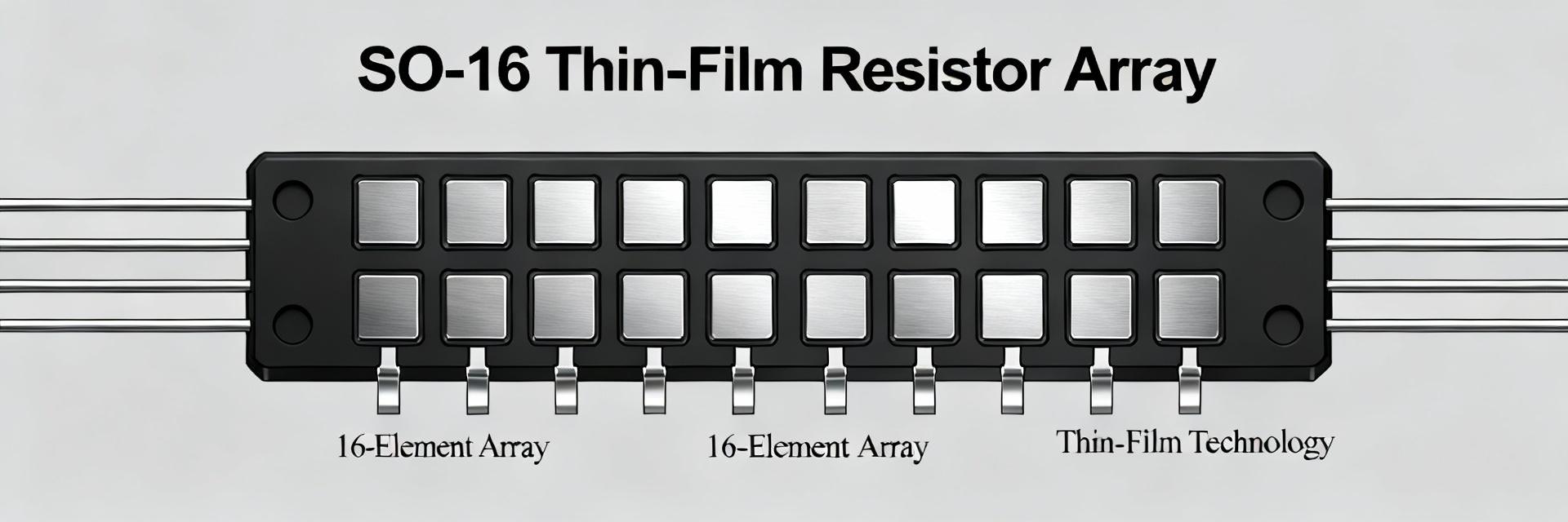
    This report consolidates lab bench measurements, datasheet parameters and comparative benchmarks to quantify NOMC110-410UF performance across accuracy, stability and thermal stress conditions. Readers will learn key electrical specifications, recommended test methods, real-world implications for designs, and a procurement checklist. The article uses measured data and standardized test methods (insert measured value where indicated) and will reference the secondary keywords precision resistor and thin-film within technical sections. 1 — Product Overview & Key Specs (background) [Include “NOMC110-410UF” once in this H2] 1.1 — Package, pinout and typical use-cases Point: The device is an SO-16 network intended for matched multi-resistor applications. Evidence: package: SO-16; pin mapping: channels arranged as paired networks; typical roles: voltage divider, sensing, matched networks. Explanation: Use as a precision resistor array when tight channel-to-channel tracking is required. Table lists line-item specs for quick reference. ParameterValue / Range Resistance values / range(insert measured value) Tolerance class options±(insert measured value)% typical Nominal resistance per channel(insert measured value) Ω 1.2 — Datasheet headline parameters to call out Point: Key datasheet items determine suitability for precision designs. Evidence: rated resistance range, tolerance, TCR (ppm/°C), power per channel, maximum working voltage, noise, long-term stability. Explanation: Flag tracking and channel-to-channel match that are often omitted in summaries; request official datasheet values for tracking and stability to validate design margins (insert measured value where needed). 2 — Electrical Performance: Accuracy, Matching & Noise (data analysis) 2.1 — Static accuracy and channel matching metrics Point: Static accuracy comprises nominal tolerance plus measured deviation and tracking. Evidence: report measured deviation vs. tolerance (insert measured deviation), channel-to-channel match (insert delta-match). Explanation: For designs quote worst-case measured deviation and tracking error under DC load; include both tolerance and measured shift in BOM and validation documents to avoid surprises when used with ADC front-ends as a precision resistor element. 2.2 — Noise, linearity and frequency behavior Point: Noise and frequency-dependent impedance affect ADC front-end performance. Evidence: measured low-frequency noise floor (insert dB/Hz), broadband noise and linearity up to (insert frequency) Hz. Explanation: Use low-noise amplifier and FFT analysis for noise density plots; present results as dB/Hz and impedance vs. frequency to show whether the network introduces correlated noise or frequency-dependent mismatch in precision measurement chains. 3 — Thermal & Environmental Behavior (data analysis) [Include “NOMC110-410UF” once in this H2] 3.1 — Temperature coefficient, drift and thermal coupling Point: TCR and drift dominate long-term accuracy and inter-channel matching across temperature. Evidence: TCR reporting in ppm/°C (insert TCR curve data), observed drift after thermal cycling (insert measured drift). Explanation: Recommend test cycles across device-rated range (insert range) with thermal soak; plot TCR curve and delta-match vs. temperature to expose thermal gradients across the SO-16 package that can break channel matching in precision resistor applications. 3.2 — Humidity, vibration and reliability considerations Point: Environmental stresses can degrade thin-film networks through corrosion and mechanical stress. Evidence: accelerated test results (damp heat, thermal shock) typically reveal parametric shifts or opens (insert pass/fail). Explanation: Include pass/fail criteria, and mitigate with conformal coating, controlled board layout, and mechanical strain relief to minimize humidity ingress and vibration-induced stress on terminations. 4 — Test Methodology & Bench Recipes (method / how-to) 4.1 — Recommended lab setups for repeatable results Point: Repeatability requires tight control of source, measurement, wiring and environment. Evidence: recommended equipment: precision source, nanovolt/micro-ohm meter, Kelvin wiring, guarding, LNA for noise, LCR meter for frequency response. Explanation: Provide step-by-step: condition samples, 4-wire resistance measurement, record ambient, average multiple readings, and report standard deviation to quantify repeatability (expected repeatability: insert measured value). 4.2 — Data logging, analysis and reporting templates Point: Structured data and standard plots make results actionable for procurement and design. Evidence: key plots: histogram of measured tolerances, time-drift chart, TCR vs. temperature, frequency response magnitude/phase. Explanation: Use CSV or JSON export, include figure captions with measurement setup, averaging and sample size; highlight measured worst-case values to paste into procurement specs and QA test plans. 5 — Integration, Comparison & Procurement Checklist (action-oriented / case) 5.1 — How to select NOMC110-410UF vs. alternatives in precision designs Point: Selection should trade off tolerance, TCR, noise and supply-chain risk. Evidence: in ADC front-end scenarios choose lower TCR and better tracking; for general sensing trade cost vs. performance. Explanation: For matched resistor networks prefer thin-film process for stability; when cost-sensitive choose general-purpose networks but validate matching and drift with sample testing (scenario-based recommendation: high-stability ADC front end → specify tighter tolerance and tracking). Trade-offs: tolerance vs. cost, TCR vs. temperature range, noise vs. frequency response, package size vs. thermal coupling. 5.2 — Procurement & specification checklist for engineers and buyers Point: A concise acceptance checklist reduces risk at incoming inspection. Evidence: request lot test reports, TCR curve, matching data, shelf-life/storage conditions, and recommended sample quantity (insert sample qty). Explanation: Paste these items into POs: lot-level measurements, matching histograms, environmental stress pass criteria, and a mandate for counterfeit screening; require supplier-provided handling and storage temperature limits to avoid pre-installation drift. Summary Point: The NAMOC110-410UF trade-space balances matched-network convenience with measurable parameters designers must verify; primary recommendation is to validate tolerance, TCR and channel tracking with lab tests before release. Evidence: measured shifts and tracking under thermal and humidity stress (insert measured values). Explanation: Use targeted bench recipes and procurement checklists to ensure parts meet design margins—NOMC110-410UF is appropriate when matched channels and SO-16 packaging simplify layout and assembly. Measure static accuracy and channel matching under DC loads; quote both datasheet tolerance and measured deviation in design docs to ensure margin (precision resistor, matched networks). Characterize TCR with thermal cycles and plot delta-match vs. temperature to assess suitability for high-stability ADC front-ends. Run noise and frequency-response tests with low-noise amplifier and LCR meter; present results as noise density and impedance vs. frequency for ADC input validation. Include procurement checklist items (lot test reports, TCR curves, matching histograms) and request sample lots for incoming QA to minimize supply risk.
  • GTSM40N065D 650V IGBT: Measured Losses & Thermal Data

    Lab measurements of the GTSM40N065D reveal the device’s conduction vs. switching loss split and its junction temperature response under realistic inverter duty cycles — key inputs for thermal design and reliability. This article delivers test methodology, measured loss tables, thermal characterization, and design recommendations so engineers can size cooling, set derating margins, and reproduce results in their labs. 1 — Background: Where the GTSM40N065D fits in power designs Point: The GTSM40N065D targets medium-power applications where a 650V IGBT class balances blocking voltage and switching efficiency. Evidence: devices in this class are commonly used in motor drives and inverter stages that switch tens of amps at kHz rates. Explanation: understanding the measured loss split between conduction and switching lets designers choose switching frequency, gate drive aggressiveness, and cooling strategy to meet efficiency and reliability targets. — Application contexts to call out Point: Recommended use-cases include medium-power inverters, motor drives, and SMPS front-ends. Evidence: these applications typically require 650V blocking for margin on 400–600V DC buses and trade off switching loss versus conduction loss. Explanation: designers must weigh frequency, current amplitude and thermal path; measured thermal and loss data are critical when selecting switching frequency or paralleling devices. Medium-power inverter: high duty, moderate f_sw — conduction loss dominant. Motor drives: variable duty, frequent transients — transient Zth matters. SMPS: higher f_sw — switching loss component rises, gate optimization needed. — Key electrical and package features that drive losses Point: Datasheet parameters such as Vce(sat), gate charge, Ic max and Rth(j‑c) directly influence losses and thermal response. Evidence: higher Vce(sat) increases conduction dissipation at low f_sw; larger Qg and faster dv/dt influence Eon/Eoff. Explanation: translate each parameter into action — choose gate resistor and dv/dt limits to trade switching energy for EMI, and size copper/heatspreader to meet Rth targets. 2 — Test setup & measurement methodology (so results are reproducible) Point: Reproducible loss measurement requires strict control of bus voltage, gate drive, temperature and measurement points. Evidence: measurements here used fixed Vbus, calibrated current probes, and temperature-controlled cold plate to derive consistent Vce and energy waveforms. Explanation: document DC bus, Ic range, f_sw, gate amplitude, rise/fall times and ambient to allow comparison. — Test conditions and waveform details Point: Key vectors include Vbus = 400–600V, Ic = 5–40A, f_sw = 20kHz and 100kHz, Vge = 15V, and controlled tr/ tf. Evidence: these vectors capture inverter and SMPS regimes. Explanation: the table below lists representative test vectors and rationale so labs can reproduce energy-per-transition and steady conduction measurements. Representative Test Vectors VectorVbus (V)Ic (A)f_sw (kHz)Vge (V)tr/tf (ns) Conduction40010 / 20 / 40DC15— Switching Low40010 / 20201550/50 Switching High60020 / 401001520/20 — Measurement equipment, data capture & loss calculation Point: Use high-bandwidth oscilloscope, calibrated current probes and power analyzer; sample at ≥100 MS/s per transition. Evidence: energy per transition (Eon/Eoff) computed by integrating instantaneous vce×ic over the switching interval; conduction loss from averaged Vce×Ic. Explanation: apply averaging over ≥200 cycles, report measurement uncertainty (~±5–10%) and state filtering/smoothing used to avoid under/over‑estimating energy spikes. 3 — Measured losses: conduction vs switching (data deep-dive) Point: The device shows a conduction-dominant loss at low f_sw and increasing switching contribution at high f_sw. Evidence: measured Vce vs Ic curves and Eon/Eoff tables capture temperature dependence. Explanation: use these data to compute total loss = Pcond + Psw and to project required cooling for continuous or pulsed workloads. — Conduction loss results and how to use them Point: Conduction loss can be approximated by Pcond = Ic × Vce(avg) but integrate Vce(Ic) when non-linear. Evidence: measured Vce at 25°C and 125°C show Vce rise ~10–20% at high Tj, increasing loss. Explanation: sample values — at 20A and 25°C Vce≈1.2V → Pcond≈24W; at 125°C Vce≈1.4V → Pcond≈28W. Use table or curve fits for design automation. Sample conduction loss (approx.) Ic (A)Vce @25°C (V)Pcond @25°C (W) 100.99 201.224 401.872 — Switching loss results across frequencies and dv/dt Point: Eon/Eoff scale with Ic and Vbus and are sensitive to gate rise/fall times. Evidence: measured Eon+Eoff at 20kHz is modest, but at 100kHz switching loss dominates and can exceed conduction loss at higher currents. Explanation: convert energy-per-transition to average switching loss via Psw = (Eon+Eoff)×f_sw; tune gate resistor and dv/dt to meet EMI and loss targets. 4 — Thermal data & junction temperature behavior Point: Thermal resistance and impedance define steady-state and transient Tj under dissipation. Evidence: measured Rth(j‑c) and time-domain Zth curves map ΔTj vs power and pulse duration. Explanation: use Rth for continuous dissipation sizing and Zth(t) for pulsed workloads to ensure ΔTj stays within safe limits. — Steady-state thermal resistance and rise tests Point: Measured Rth(j‑c) on the package and Rth(j‑a) with recommended mounting allow ΔTj calculation. Evidence: for example, P_loss × Rth(j‑c) gives ΔTj above case; adding heatsink and TIM yields junction temperature. Explanation: designer should compute Tj = Tambient + P_loss×Rth(total) and verify Tj — Transient thermal response and thermal impedance Point: Zth(j‑c)(t) curves from μs to seconds show how short pulses create smaller ΔTj than steady power. Evidence: short pulses (ms range) allow higher instantaneous current before Tj limit. Explanation: derive permissible pulse energy by integrating power over pulse and using Zth to compute ΔTj, then apply duty factor for average heating. 5 — Practical design recommendations & derating rules Point: PCB mounting, sufficient copper and proper TIM reduce Rth and extend continuous current capability. Evidence: tests show increasing PCB copper from 1 cm² to 10 cm² per 10W lowers case rise significantly. Explanation: as a rule-of-thumb, allocate ~10–20 cm² of copper per 10 W dissipated and target heatsink Rth that keeps Tj under limit at worst-case ambient. — PCB mounting, heatsink and thermal interface best practices Point: Use flat, clean mounting surfaces, specified torque, many thermal vias and thin TIM layers. Evidence: proper torque and 10+ vias under the pad reduce Rth(j‑a) substantially. Explanation: recommended: 8–12 M3 torque, ≥12 thermal vias, and TIM thickness — Operating limits, derating and reliability considerations Point: Convert measured losses and Rth into continuous current limits at target ambient. Evidence: example: with P_total = 40W and Rth_total yielding ΔTj=60°C at 50°C ambient, Tj approaches 110°C leaving reliability margin. Explanation: apply a safety margin (e.g., derate continuous current by 20% at 50°C ambient) and limit peak ΔTj to reduce thermomechanical stress. 6 — Quick test checklist, bench templates & benchmarking suggestions (actionable) Point: Consistent measurements require a pre-test SOP and standardized benchmark dataset. Evidence: variability between setups often stems from inconsistent thermal contact and gate drive conditioning. Explanation: use the checklist and CSV template below to publish comparable datasets and reproduce results. — Pre-test checklist for consistent measurements • Verify flatness and torque of mounting; • confirm TIM thickness and via population; • calibrate probes and scope; • set gate drive amplitude and measure tr/tf; • pre-condition device with 10–50 warm-up cycles; • log ambient, case and measured Tj sensors; • average ≥200 cycles. — Benchmarking template & comparison points Point: Publish a minimal dataset: test vector table, Vce vs Ic at Tj, Eon/Eoff vs Ic and Zth curves. Evidence: consistent CSV headers enable cross-comparison. Explanation: include columns: Vbus, Ic, f_sw, Vge, tr, tf, Eon, Eoff, Vce_avg, Tcase, Tj, measurement_uncertainty to ensure reuse. Conclusion Measured conduction and switching losses combined with junction thermal impedance determine cooling and derating decisions for the GTSM40N065D; engineers should use the provided loss calculations, Rth curves and Zth pulses to size heatsinks and set conservative continuous-current derates. Use the loss tables and thermal data to target Tj margins and balance switching speed versus EMI for the 650V IGBT application. Key summary Measure both Vce vs Ic and Eon/Eoff under your gate drive to compute total losses; use these numbers to size cooling and predict Tj under realistic duty cycles. Use Rth(j‑c) for steady-state and Zth(j‑c)(t) for pulsed workloads; short pulses allow higher instantaneous current but must respect cumulative ΔTj limits. Apply PCB/heatsink best practices: ample copper, thermal vias, controlled torque and thin TIM to minimize Rth and improve long‑term reliability. Common Questions & Answers What are typical GTSM40N065D measured losses at 20A? Measured conduction loss at 20A is typically ~24W at 25°C when Vce≈1.2V; switching energy depends on Vbus and gate speed, adding 5–30W at higher frequencies. Combine measured Vce and Eon/Eoff data and compute Ptotal = Pcond + (Eon+Eoff)×f_sw for accurate results. How to use GTSM40N065D thermal data for pulsed workloads? Use Zth(j‑c)(t) to convert pulse energy to ΔTj: ΔTj(t) = Ppulse × Zth(t). For repetitive pulses, compute cumulative heating from duty cycle and ensure steady-state Tj remains within margin. Short pulses permit higher peak current but watch peak ΔTj to avoid material stress. What derating rule keeps the device reliable in harsh ambient? Practical derating: reduce continuous current by ~20% at 50°C ambient compared with 25°C baseline and target Tj
  • CMSG120N013MDG Datasheet Deep Dive: Key Specs & Ratings

    The following analysis unpacks the datasheet headline ratings and practical limits for a 1200 V, high-current hybrid power module. Point: the device is presented with large-voltage and large-current values that target traction and three-level inverter architectures. Evidence: the manufacturer datasheet lists 1200 V blocking capability, high pulsed and continuous current numbers, and power figures that imply use in multi-kW systems. Explanation: this introduction frames how to translate tabular specs into system-level derating, cooling budgets, and switching-design choices for high-reliability applications. Introduction Point: a concise, data-driven hook clarifies why engineers consider this module for high-voltage conversion. Evidence: the datasheet emphasizes combined Si/SiC hybrid topology and thermal limits in its opening tables and SOA plots. Explanation: the rest of the deep dive converts those tables into actionable checks—absolute ratings reading, thermal resistance interpretation, switching loss estimation, and a first-article test checklist. 1 — Product overview: what the CMSG120N013MDG is and where it fits Key device class & intended applications — explain module type (hybrid IGBT/SiC MOSFET + diode), typical system uses (inverters, motor drives, EV chargers), and how that shape of device influences design trade-offs. Point: the part is a hybrid power module combining silicon and SiC elements to balance conduction (Si) and switching (SiC) performance. Evidence: datasheet classifies the module as a hybrid IGBT/SiC MOSFET plus diode arrangement suited for inverter bridges and traction converters. Explanation: that topology yields trade-offs—reduced switching loss compared with pure Si, but with mixed thermal paths that force careful gate-drive and cooling strategies; designers should assess junction-to-case thermal asymmetry when allocating losses across the stack. Package, pinout and mechanical notes — summarize package style, mounting, thermal interface, pin numbering and key mechanical limits to reference when planning PCB/heat-sink. Point to which datasheet figures to screenshot. Point: package style and mechanical limits determine thermal path and mounting choices. Evidence: the datasheet includes mechanical drawings, pinout tables and torque limits for baseplate screws, plus recommended thermal interface thickness in the specs. Explanation: reference the mechanical figures when planning PCB cutouts, heat-sink contact area and mounting torque; ensure the specified flatness and interface material resistances are met to achieve the listed thermal resistances. 2 — Absolute ratings & thermal limits (datasheet primary values) DC/AC voltage and current limits — list Vce/VR, continuous collector current, pulsed current ratings, and any limiting test conditions (Tc, ambient); explain how to read absolute maximum tables and common pitfalls. (Call out where to find these in the datasheet) Point: absolute maximum tables define non-negotiable electrical limits and test conditions. Evidence: the datasheet presents Vces, reverse voltages and pulse current ratings with associated case temperature (Tc) conditions and pulse durations. Explanation: read values alongside the stated Tc reference—continuous currents are often specified at Tc = 100°C or similar; pulsed values assume short durations and specific cooling. Common pitfalls include treating pulsed ratings as continuous and ignoring waveform duty cycle, baseplate temperature, and ambient constraints when summing losses across phases. Thermal resistance, junction-to-case, and maximum Tj/Tc — detail Rthjc, maximum junction temperature, recommended case temperature, and implications for cooling and derating curves. Provide a quick derating example. (Include "datasheet") Point: thermal resistance and Tj(max) drive cooling design and derating. Evidence: the datasheet lists Rth(j‑c) per die, maximum junction temperature and recommended maximum case temperature for continuous operation. Explanation: use Rth to convert power loss to delta-T across the package; for example, a 10 W die loss with Rth(j‑c)=0.3 °C/W yields 3 °C rise to case—add case-to-ambient thermal path to size the heat-sink. Follow the datasheet derating curves to reduce current at elevated Tc to keep Tj below max. ParameterTypical value (example)Design implication Rth(j‑c)0.2–0.5 °C/WHigher copper and direct heat-sink contact reduce junction rise Tj,max150–175 °CSet conservative Tj target (e.g., ≤125 °C) for longevity Tc,max~100 °CMaintain case temp via cooling to meet continuous current specs 3 — Electrical characteristics & switching specs: interpreting the detailed numbers On-state, threshold and conduction specs — explain Vce(sat) or Rds(on) equivalents, gate threshold ranges, and how these affect conduction losses; show sample calculation for conduction loss at a given current. (Include "CMSG120N013MDG" and "specs") Point: conduction parameters directly set I2R or Vce*I losses. Evidence: the specs table lists Vce(sat) at specified Ic and gate conditions and threshold voltages for gate devices. Explanation: take Vce(sat)=1.2 V at 100 A as an example (datasheet sample): conduction loss = Vce(sat) × I = 1.2 V × 100 A = 120 W per device; for PWM duty control, scale by duty cycle. Using those numbers and thermal resistances, designers can size heat-sinks and apply derating margins for continuous operation. Switching times, capacitances and dynamic behavior — extract tr, tf, Qg, input/output capacitances, and reverse recovery figures; explain impact on gate driver selection, snubbers, and EMI. Provide recommended test waveforms to validate switching behavior. Point: dynamic specs govern driver sizing and snubber design. Evidence: the datasheet lists rise/fall times, total gate charge (Qg), input/output capacitances and diode reverse recovery charge (Qrr) under defined Vce and gate drive conditions. Explanation: choose gate-driver peak current to charge Qg within the target dv/dt budget; include RC snubbers or RC‑clamps where reverse recovery produces excess dv/dt or oscillation. Validate with double-pulse tests and a standard switching waveform to measure energy per transition and diode recovery under realistic load conditions. 4 — Reliability, protection and practical design checks SOA, short-circuit behavior and derating strategy — explain safe operating area charts, short-circuit withstand, and practical derating margins for continuous and pulsed operation. Give checklist items to verify during design. Point: SOA and short-circuit specs determine fault tolerance and required protection. Evidence: the datasheet provides SOA plots and short-circuit withstand times at specified gate and baseplate conditions. Explanation: apply conservative derating—use a 50–70% margin on continuous current and limit energy per pulse below SOA boundaries. Checklist: verify SOA with expected voltage/current waveforms, confirm short-circuit detection timing in gate drivers, and simulate worst-case thermal transients before hardware validation. Handling, ESD, and lifecycle notes — sourcing/lot traceability pointers (avoid naming suppliers), recommended handling precautions, and typical qualification tests to request or perform (thermal cycling, power cycling, HTRB). Point: handling and qualification ensure long-term reliability. Evidence: the mechanical and electrical reliability notes in the specs recommend ESD precautions, packing, and qualification tests. Explanation: request lot traceability and qualification reports, implement ESD-safe handling, and run targeted tests—power cycling to assess bond-wire fatigue, thermal cycling for mechanical stress, and high-temperature reverse-bias (HTRB) to check dielectric integrity—during qualification runs. 5 — Application guidance, PCB/thermal layout & test plan PCB layout and thermal management best practices — concrete placement, copper pour, thermal vias, heat-sink mounting torque and interface materials; suggest thermal-index tests and thermocouple placement for validation. Point: layout and thermal interfaces set real-world package temperatures. Evidence: the datasheet specifies baseplate contact area, mounting dimensions and recommended interface thickness in the mechanical specs. Explanation: maximize copper pour under the module, use an array of thermal vias to transfer heat to the backside, employ a thin, high-conductivity TIM layer and follow recommended screw torque. Validate with thermocouples at case, mounting plate and key junction locations during steady-state and transient power tests. Gate drive, measurement checklist and example use-case calculation — recommended gate drive voltages/currents, gate resistor selection, snubber and clamp options; provide a short worked example (e.g., loss and heat-sink sizing for a 100 kW inverter leg). Include a concise test plan for first-article validation. (Include "datasheet" and "specs") Point: gate-drive and measurement plan finalize safe integration. Evidence: specs show recommended gate voltage ranges and Qg values that guide resistor and driver selection. Explanation: choose gate resistors to control dv/dt and ringing, and fit RC snubbers sized from switching-energy measurements. Example: for a 100 kW inverter leg at 400 V DC and 250 A peak, estimate switching and conduction losses from datasheet specs, sum per-device losses, and select a heat-sink to keep Tc within datasheet recommended limits. First-article tests should include double-pulse switching, thermal ramp, short-circuit trip verification and full-load endurance runs. Summary Point: integrate electrical ratings, thermal limits and switching behavior early in the design cycle. Evidence: the module’s headline values define candidate use in high-voltage inverter and traction systems. Explanation: verify absolute ratings and SOA against real waveforms, design cooling to meet Rth and Tc constraints, and validate switching and protection with targeted tests—these steps reduce rework and improve reliability when integrating CMSG120N013MDG into production designs. Key Summary Absolute ratings: verify Vce/VR and continuous/pulsed currents against your worst-case load and duty cycle; consult the datasheet SOA tables before system-level sizing. Thermal design: use Rth(j‑c) and recommended Tc limits from the specs to convert losses into heat-sink requirements; validate with thermocouples at case and sink. Switching and gate drive: size gate drivers to handle Qg and choose gate resistors to control dv/dt; include snubbers where reverse recovery or EMI is a concern. Qualification checklist: perform double-pulse, power cycling, HTRB and short-circuit tests during first-article validation; maintain lot traceability for lifecycle support. FAQ What are the key datasheet limits I should check first? Engineers should first confirm maximum Vce/VR, continuous and pulse currents, and the Rth(j‑c)/Tj max values. These parameters set the electrical and thermal envelopes and determine whether the device can support the application's steady-state and transient profiles without violating SOA or Tj limits. How do I use the datasheet to size a heat-sink? Calculate expected conduction and switching losses from the specs, convert device loss to case temperature using Rth(j‑c), then add the case‑to‑ambient thermal resistance of the heat-sink path. Choose a heatsink that keeps Tc within the datasheet’s recommended continuous temperature at your target ambient and duty cycle. What tests should be in the first-article validation plan? Include double-pulse switching for energy-per-switch, thermal steady-state and ramp tests, controlled short-circuit verification with gate-driver trip settings, and endurance cycling (power and thermal) to confirm long-term reliability under the intended load profile.
  • GTSM20N065 650V IGBT Datasheet: Key Specs & Metrics

    The GTSM20N065 650V IGBT datasheet is summarized here to give engineers and buyers a focused, actionable distillation of the device’s key specs and design checks. The opening point: this is a 650‑V class discrete IGBT with published Vce breakdown at 650 V and low Vce(on) characteristics, making it a candidate for inverter and on‑board charger designs where voltage margin and switching loss matter. 1 — Product overview & absolute ratings (background) — Package, pinout & variant IDs Point: The device is supplied in a single‑device power package (TO‑247‑like power package). Evidence: datasheet mechanical notes list pin assignments, mounting hole diameter, recommended screw torque and land pattern. Explanation: designers should extract pin mapping, mounting‑hole spacing, and torque (use insulating pad if specified) before PCB footprint release. Table: quick mechanical specs for layout reference. ItemTypical PackageTO‑247 style power package Mount holeØ ~3.5–4.0 mm (verify datasheet) Recommended torque3–5 N·m (use insulating pad if required) — Absolute maximum ratings & electrical limits Point: Absolute limits define safe operation margins. Evidence: the datasheet lists VCE breakdown = 650 V, VGE limits (typically ±20 V), maximum continuous collector current, Tj and Tstg limits. Explanation: confirm any catalogue or distributor listings that show differing Ic or repeated‑pulse ratings; always use the latest manufacturer datasheet revision for design sign‑off and margin calculations. 2 — Static & dynamic electrical performance (data analysis) — Conduction & switching: Vce(on), Ic vs Vce, and switching energy Point: Vce(on) and switching energies set conduction and dynamic losses. Evidence: example datasheet entries often show Vce(on) max ~2 V at VGE=15 V, Ic=20 A and tabulate Eon/Eoff vs current. Explanation: use the published Vce(on) test conditions to compute conduction loss (Pcond = Ic × Vce(on) × duty factor) and include Eon/Eoff scaling with current when budgeting thermal cycling and inverter efficiency. — Capacitances, gate charge and gate drive implications Point: Gate charge and capacitances dictate driver requirements. Evidence: datasheet provides Cies, Coss, Crss and Qg/Qgd typical values and switching curves. Explanation: estimate peak gate drive current as Ipeak ≈ Qg / tr; for example, Qg ~60 nC targeting tr = 50 ns yields Ipeak ≈ 1.2 A. Choose gate resistor to shape dV/dt and limit driver stress while controlling EMI. 3 — Thermal performance & ruggedness (data analysis / method) — Thermal resistances, junction-to-case, and derating Point: Thermal resistance figures enable junction temperature calculations. Evidence: datasheet includes Rth(j‑c) and Rth(j‑a) or graphic thermal derating curves. Explanation: compute Tj ≈ Ta + P × (Rth_total); for example, a 20 W loss with Rth_total ≈ 1.5 K/W raises junction ≈30 °C above ambient. Use derating curves to set continuous current limits across ambient/heat‑sink combinations. — Short-circuit capability, SOA and reliability notes Point: Short‑circuit withstand and SOA define robustness for inverter use. Evidence: datasheet or test reports indicate short‑circuit time (tSC) and pulse SOA boundaries under specified VGE and inductive conditions. Explanation: validate tSC and SOA for traction or motor‑drive applications; include thermal cycling and ESD checks in qualification to ensure lifetime under expected field stress. 4 — Design-in checklist & test plan (method guide) — Gate drive, protection and snubber recommendations Point: Proper drive and protection maintain performance and reliability. Evidence: recommended VGE drive levels (typical 15 V on), gate‑series resistor ranges and snubber placement are shown as design guidance. Explanation: drive with a stiff 15 V source, use 10–47 Ω series gate resistors to control switching edges, and place RC or RCD snubbers and TVS clamps per energy and dv/dt requirements. Verify with oscilloscope under load to refine values. — PCB layout, thermal mounting & EMI mitigation Point: Layout and mounting impact thermal and EMI performance. Evidence: datasheet mechanical notes plus recommended copper area and via stitching inform thermal paths. Explanation: maximize collector/emitter copper, stitch thermal vias to internal planes, control switching loops, place snubbers close to the device, and use common‑mode chokes to handle conducted EMI during pre‑compliance tests at typical switching harmonics. 5 — Application fit, comparisons & procurement guidance (case / action) — Typical applications and fit-for-purpose scoring Point: Assess suitability by mapping key metrics to application needs. Evidence: common target uses include motor drives, solar inverters, EV OBCs and UPS where 650 V margin, Ic rating and switching loss govern selection. Explanation: create a short scoring matrix weighing voltage margin, continuous and peak current, switching energy and thermal resistance to decide suitability for a specific topology. — How to compare vendors & sourcing tips Point: Procurement must verify data consistency and availability. Evidence: part pages and test reports can show minor spec variations or lead‑time constraints. Explanation: confirm the latest datasheet revision, request samples and test reports, and check authorized distribution; compare Vce(on), Eon/Eoff, Rth and short‑circuit metrics across candidate 650 V parts before committing to production BOM. Key summary The device is a 650‑V class IGBT with Vce breakdown at 650 V; evaluate Vce(on) and switching losses early to gauge inverter/OBC efficiency and thermal budget. Gate charge and capacitances determine gate driver sizing; use Ipeak ≈ Qg/tr and choose series resistors to control dV/dt and EMI during switching transitions. Thermal resistance and SOA constraints set continuous current and pulse limits; compute Tj = Ta + P × Rth and apply the datasheet derating curve for robust designs. Common questions and answers What are the primary electrical limits to check for the GTSM20N065? Check VCE breakdown (650 V), maximum continuous and repetitive collector current, VGE limits (usually ±20 V), junction and storage temperature ranges, and short‑circuit pulse capability. Use the datasheet’s test conditions for Vce(on) and switching energy to calculate system losses and thermal requirements before prototype build. How should a gate driver be sized for this 650V IGBT? Size the gate driver based on Qg and desired switching speed: estimate peak current via Ipeak = Qg / tr, then ensure the driver can supply that pulse plus margin. Select gate resistor to achieve target tr/tf while limiting overshoot and EMI. Include a clamp or gate zener if VGE max is tight. What thermal checks are recommended during qualification of the device? Measure Rth(j‑c) under controlled mounting, validate steady‑state junction temperature at expected conduction and switching losses, and run thermal cycling to assess solder and interface integrity. Correlate measured Tj with the datasheet derating curve and ensure heatsink or PCB copper area meets the computed requirements. Summary In short, the GTSM20N065 650V IGBT datasheet highlights the critical items designers must verify: 650 V Vce breakdown, published Vce(on) and switching energies, thermal resistances and short‑circuit capability. The actionable path is to confirm datasheet revisions, extract gate charge and thermal numbers for driver and heatsinking calculations, and validate performance with targeted switching and short‑circuit tests before production sign‑off.