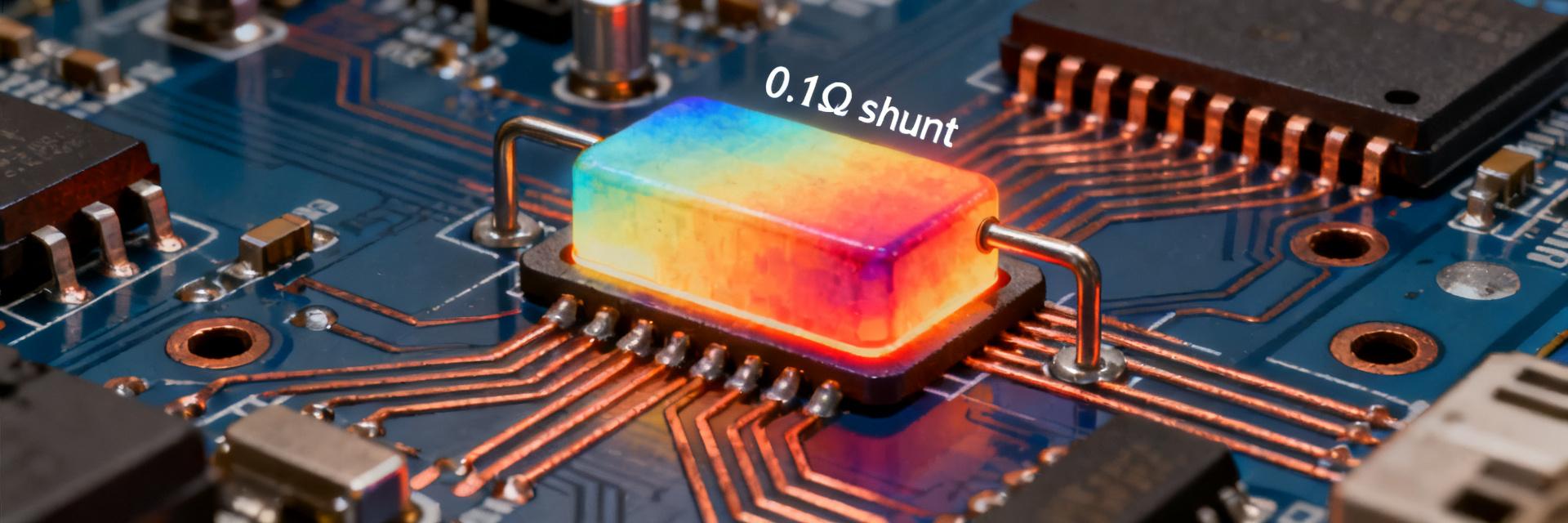
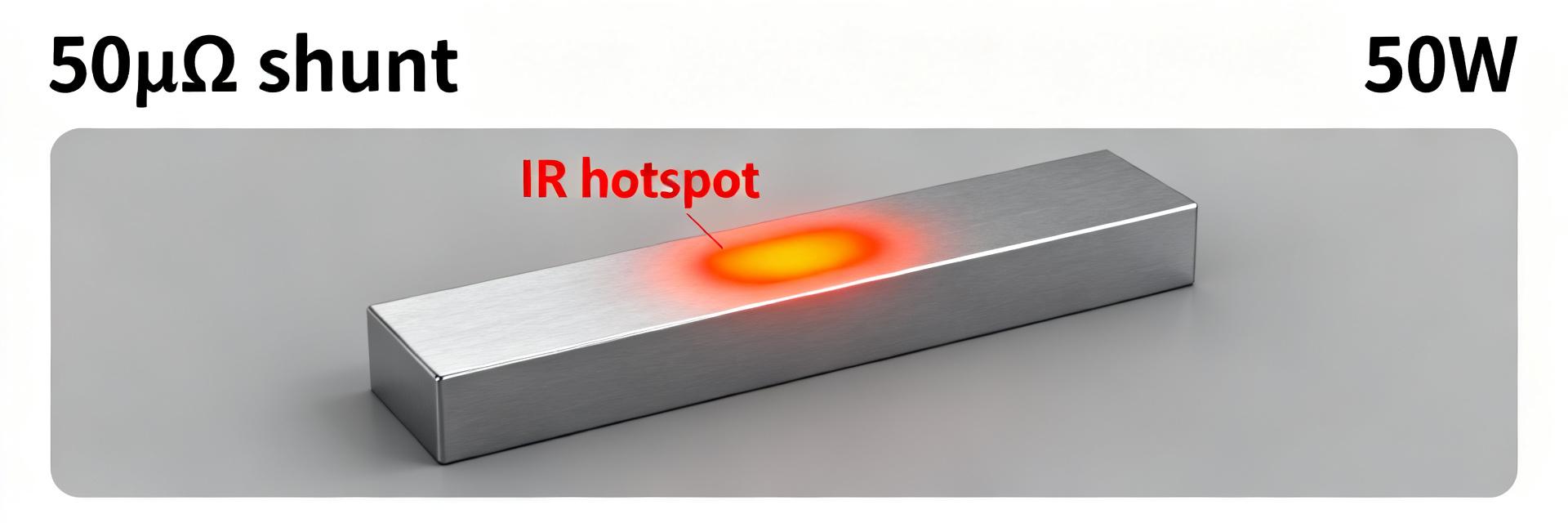
50µΩ Shunt Performance Analysis: Measured Specs & Limits
In controlled 4‑wire bench tests, nominal 50µΩ shunts exhibit sub‑0.5% initial tolerance across a 20‑unit sample but can show up to 3.5% drift after prolonged high‑power stress — a gap that makes or breaks high‑current measurement accuracy. This article presents measured specs, identifies hard limits, and gives practical testing and design guidance for engineers specifying or measuring a 50µΩ shunt.
The goal is actionable: reproducible measurement methods, a compact specs template, thermal and long‑term limits, and checklists engineers can use to qualify parts and designs for battery packs, motor drives, and power electronics.
Background — Why a 50µΩ shunt matters in high‑current sensing
Typical applications & performance targets
Point: Low‑ohm shunts are chosen where measurement loss must be minimized while preserving millivolt‑level sense voltage. Evidence: common uses include battery management systems, EV motor controllers, power supplies, and pack current measurement where continuous currents range from tens to several hundred amps. Explanation: Engineers typically target overall current measurement accuracy of 0.1–1% RMS; a 50µΩ shunt yields 5 mV at 100 A, balancing power loss and resolution when paired with low‑noise amplifiers.
Typical construction, materials & packaging
Point: Construction and thermal mass determine TCR and stability. Evidence: foil, metal‑strip, and block shunts use alloys optimized for low TCR; welded or screw terminals change thermal impedance. Explanation: Higher thermal mass reduces transient rise but may mask localized annealing; choice of alloy and terminal design sets initial tolerance, TCR (ppm/°C), and susceptibility to mechanical fatigue.
Data Analysis — Measured specs: resistance, TCR, power rating, and noise
Measurement methodology & test setup
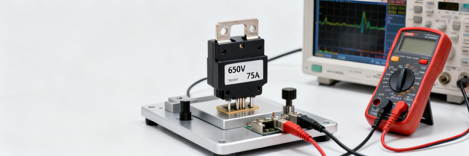
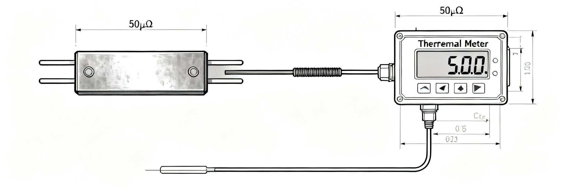
Point: Reproducible 4‑wire Kelvin measurement is mandatory for sub‑1% R accuracy. Evidence: use a precision current source with <0.01% stability, a nanovoltmeter with nV resolution, and a low‑thermal‑EMF fixture; thermal equilibrium must be allowed between current steps. Explanation: Record R at multiple steady currents and ambient temps, estimate uncertainty (type B for instrument specs, type A from repeats), and report combined expanded uncertainty at 95% confidence.
Typical measured metrics & statistical spread
Point: Report R, repeatability, TCR, thermal rise, and power rating with confidence bounds. Evidence: a compact template below standardizes reporting so comparisons are meaningful. Explanation: Present resistance vs current and vs temperature plots and include 95% confidence spreads to show population scatter and unit‑to‑unit variability.
| Parameter | Test Points | Example Result | Notes |
|---|---|---|---|
| Nominal R | 1 A, 10 A | 50.2 µΩ ±0.4% | 4‑wire, 20 units |
| Short‑term repeatability | Repeated 10 A steps | ±0.08% | n=20, 5 repeats |
| TCR | −20°C → 80°C | 55 ppm/°C | Linear fit |
| Thermal rise | I^2R curve | ΔT = 5°C @ 100 A | θJA measured |
| Power rating | ΔT limit 100°C | Max continuous 40 W | Ambient 25°C, free air |
Limits — Performance boundaries: thermal, electrical, and long‑term drift
Thermal limits & derating curves
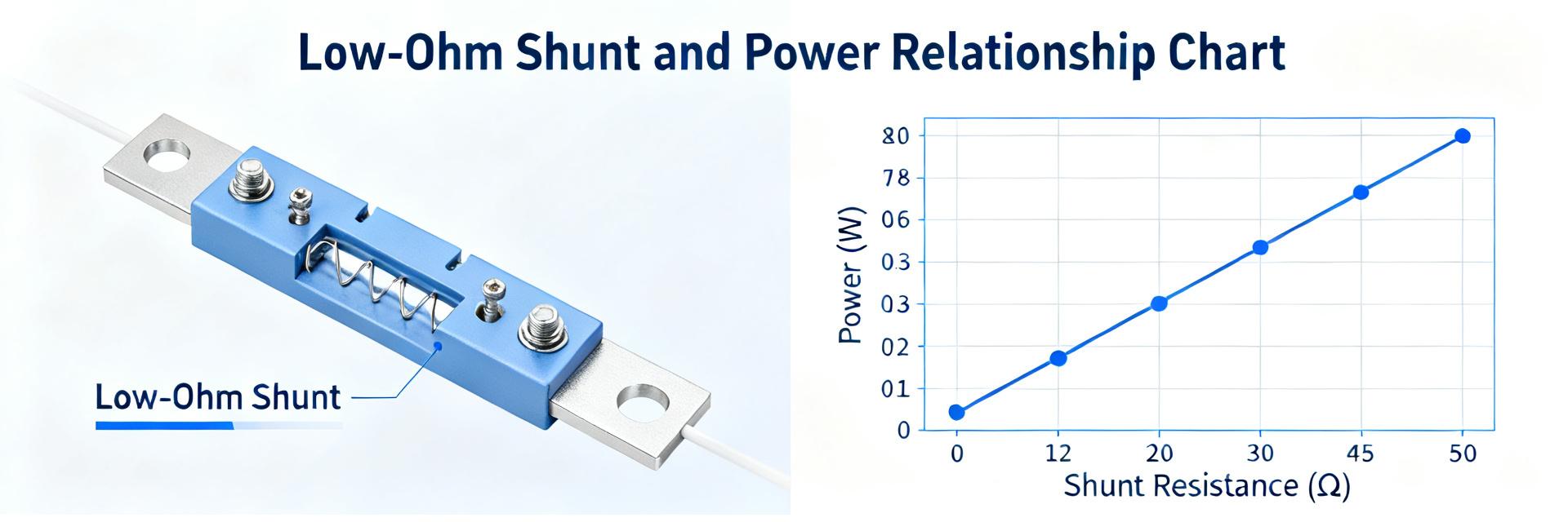
Point: Thermal limits derive from I^2R heating and thermal resistance to ambient. Evidence: P = I²R; for a 50µΩ shunt at 200 A, P = 200²×50e‑6 = 2.0 W; multiply by θJA to estimate ΔT. Explanation: Use measured θJA to build derating curves showing continuous current vs ambient for a chosen ΔT limit; account for enclosure, solder joints, and PCB copper which alter θJA and require derating for continuous operation.
Long‑term stability, mechanical fatigue & environmental limits
Point: Drift sources include annealing, contact changes, solder creep, and vibration. Evidence: accelerated tests (thermal cycling, current soak) reveal percent‑level shifts over hundreds of cycles; mechanical stress at terminals can add contact resistance. Explanation: Specify lifecycle margins (e.g., 5% over expected lifetime), require stress reports, and design mechanical strain relief to prevent terminal fatigue and resistance jumps.
Methods — Best practices for measuring and integrating low‑ohm shunts
Precise measurement techniques (4‑wire, bridge, compensation)
Point: Choose measurement topology to match required uncertainty. Evidence: 4‑wire DC measurements avoid lead errors; AC bridge or differential amplifier with offset compensation reduces low‑frequency drift. Explanation: Implement Kelvin sense wiring, guard traces for leakage, use recommended test currents (large enough to exceed instrument noise but below thermal limits), and allow settling times proportional to thermal time constant before recording.
PCB layout, grounding, and connector considerations
Point: Layout dictates measurement integrity. Evidence: star returns, thick copper pours, short sense traces and separate analog ground reduce parasitics and thermal EMFs. Explanation: Route sense traces away from power flows, use low‑thermal‑EMF connectors and compression terminals, and avoid reflow or excessive solder that can anneal the shunt; document assembly process limits in the spec sheet.
Case Study — Designing a battery‑management current sensor around a 50µΩ shunt
Example spec sheet & measurement summary
Point: A concise spec sheet eases supplier evaluation. Evidence: include nominal R, tolerance, TCR, rated continuous/intermittent current, thermal rise, and test conditions. Explanation: Report measured R at 10 A and 100 A, the TCR curve, thermal rise vs I², and uncertainty budget so system designers can predict measurement error and set amplifier gains and filtering accordingly.
Design tradeoffs & pitfalls encountered
Point: Common mistakes are undersized traces and ignoring thermal coupling. Evidence: in the case study, initial layout drove localized heating and 1.8% measurement error at 150 A until copper pours and sense reroute were added. Explanation: Calibrate after assembly, use calibration points across operating current range, and derate continuous current to stay within stable thermal regimes.
Actionable Checklist & Spec Guidance — How to select, test, and document a 50µΩ shunt
Selection checklist for engineers
Point: A checklist reduces omissions in procurement. Evidence: required items include nominal R and tolerance, TCR limit, rated continuous and intermittent current, thermal rise limit, lifecycle expectation, mounting constraints, and compatible measurement method. Explanation: Use the checklist to match supplier data to system requirements and to set acceptance criteria for incoming inspection and qualification testing.
Test report template & what to demand from suppliers
Point: Standardized test reports enable apples‑to‑apples comparison. Evidence: request 4‑wire R at multiple currents and temps, TCR curve, power/thermal curve, mechanical stress results, and assembly notes. Explanation: Require uncertainty statements and sample‑level data (n≥10) for statistical confidence; include installation notes that restrict soldering profiles and mounting torque to preserve spec integrity.
Summary
Measured specs that matter are nominal resistance, TCR, thermal rise, short‑term repeatability, and long‑term drift. A 50µΩ shunt can deliver sub‑percent accuracy when measured with proper 4‑wire technique and integrated with attention to thermal paths, calibration, and mechanical design. Engineers should run the specified bench tests, use the provided templates, and apply derating to ensure reliable operation across the product life.
Key summary
- Measure 4‑wire at multiple currents and temps; report R, repeatability, and uncertainty to compare suppliers and designs effectively.
- Derive thermal limits from P=I²R and measured θJA; use derating curves to set safe continuous and intermittent currents.
- Specify TCR, assembly constraints, and lifecycle margins; demand sample‑level test reports including thermal and mechanical stress data.
FAQ — Common questions about 50µΩ shunt measurement and specs
How to measure a 50µΩ shunt with sufficient accuracy?
Use a 4‑wire Kelvin fixture, a precision current source with very low ripple, and a nanovoltmeter or differential ADC with nV resolution. Select test currents that produce a sense voltage well above instrument noise but below the shunt’s thermal limit, allow full thermal settling between steps, and report combined uncertainty at 95% confidence.
What thermal rise can be expected for a 50µΩ shunt at high current?
Estimate using P = I²R and ΔT = P·θJA with measured θJA for the installed configuration. Example: at 200 A a 50µΩ shunt dissipates ≈2 W; with θJA = 25°C/W that yields ≈50°C rise. Enclosure, PCB copper, and solder joints significantly change θJA, so measure the final assembly.
What test items should be included in supplier data for a 50µΩ shunt?
Demand 4‑wire resistance at multiple currents and temperatures, TCR curve, I²R thermal rise curve, short‑term repeatability, mechanical stress results (thermal cycling and vibration), and an uncertainty budget. Include installation constraints for soldering and torque to prevent post‑assembly drift.
How does mechanical stress affect 50µΩ shunt long-term stability?
Mechanical strain from board flexing, vibration, or thermal expansion mismatch alters the resistor crystal lattice, causing localized resistance shifts. Designing mechanical strain-relief loops, optimizing torque specs, and specifying stable alloys minimize this drift.