NGW40T65H3DHPQ IGBT Datasheet Analysis: Key Specs & Trends
This datasheet analysis opens with a data-driven hook: the part lists a 650 V collector-emitter rating and a 40 A continuous current class with typical VCE(sat) in the 1.2–1.8 V range and switching energy Eoff/Eon figures suited to mid-kilohertz operation. The purpose is a practical decode of key specs and selection guidance.
Background — What the NGW40T65H3DHPQ IGBT is and why it matters
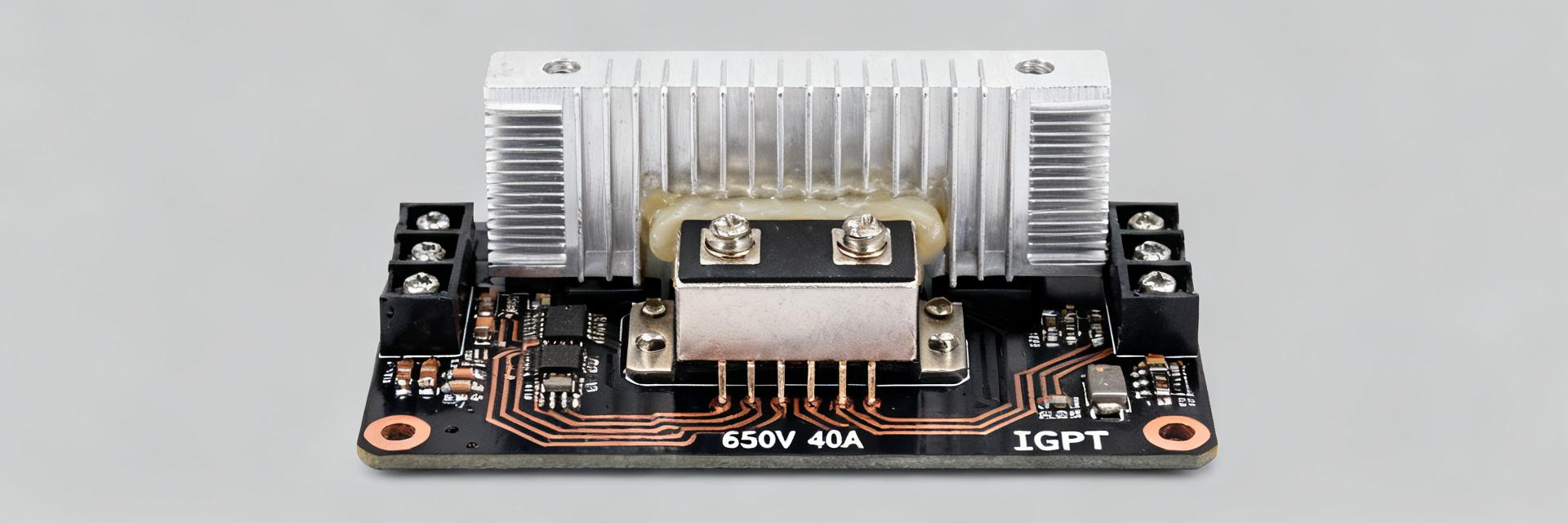
Generation & topology overview
Point: The part name implies a trench, field-stop generation optimized for lower conduction drop and faster recovery. Evidence: trench/field-stop architectures typically yield reduced VCE(sat) and controlled tail current. Explanation: That combination lowers conduction losses at high current while keeping switching-energy figures moderate, a trade-off for 650 V designs focused on efficiency and thermal budget.
Typical applications and system-level role
Point: This 650 V, 40 A class targets inverters, motor drives, power supplies, and resonant converters. Evidence: Designers select this spec class when mid-voltage margin and few-tens-of-amps continuous current are needed. Explanation: The balance of VCE(sat), switching energy, and thermal resistance makes the device suitable where compact heat sinking and moderate switching frequency are priorities; note IGBT specs guide topology choice.
NGW40T65H3DHPQ IGBT — Key datasheet specs explained (datasheet analysis)
Maximum ratings & electrical limits
Point: Read absolute maximums as non-operating limits; VCES is 650 V and gate-emitter is typically ±20 V. Evidence: Datasheet tables list continuous and pulsed IC, along with absolute derating curves for temperature. Explanation: Use derating curves for junction temperature planning; treat pulsed ratings as single-event limits and size safety margins for repetitive loads in system design.
Static conduction parameters (VCE(sat), IC vs VCE curves)
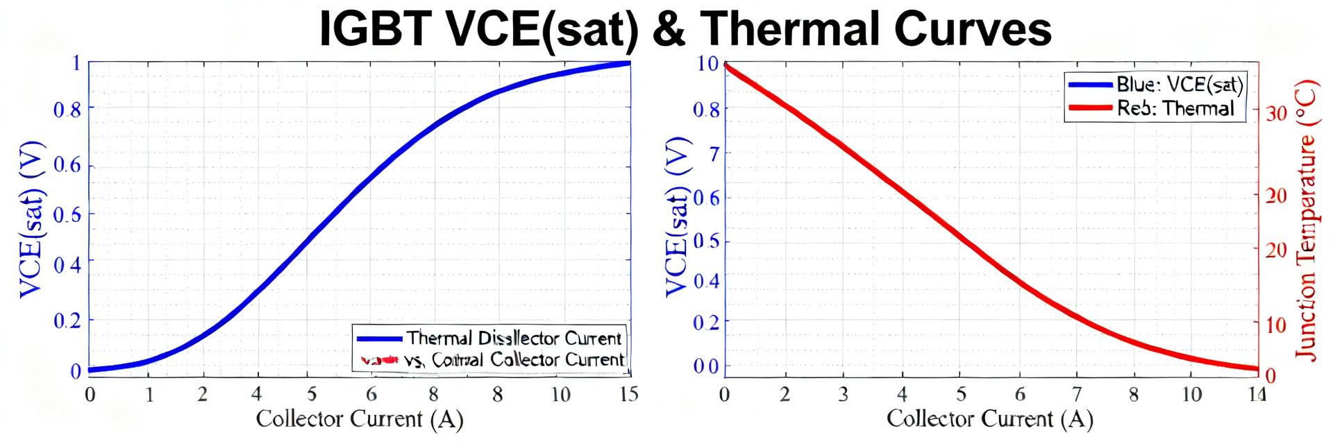
Point: VCE(sat) typical versus max influences conduction loss and heatsink sizing. Evidence: Typical VCE(sat) near 1.2–1.8 V at 40 A implies 48–72 W conduction loss per device if continuously on. Explanation: Translate curve numbers into real heatsink requirements and reserve margin—design for worst-case VCE(sat) and increased junction temperature to preserve lifetime.
Dynamic & switching specs — What the timing and charge numbers mean in practice
Switching times and energies (td(on), tr, td(off), tf, Eon/Eoff)
Point: Eon and Eoff determine switching losses at frequency; td and tf dictate waveform shape. Evidence: Datasheet lists Eoff and Eon per switching condition—use those with switching frequency to compute loss. Explanation: Calculate Pswitch ≈ f·(Eon+Eoff); pick gate drive strength to shape td and tf for acceptable EMI and loss trade-offs when estimating thermal load.
Gate charge and capacitances (Qg, Qgd, Cies, Coss)
Point: Gate charge drives gate-driver choice and affects dV/dt susceptibility. Evidence: Qg and Qgd values show required driver peak current and energy per transition. Explanation: Select driver capable of sourcing peak Igate ≈ Qg / tr and set Rgate to control di/dt and limit Miller-induced false turn-on; account for Coss in snubber and EMI planning—IGBT specs guide component choices.
Thermal, packaging & reliability considerations
Thermal resistance and junction-to-case (RthJC) implications
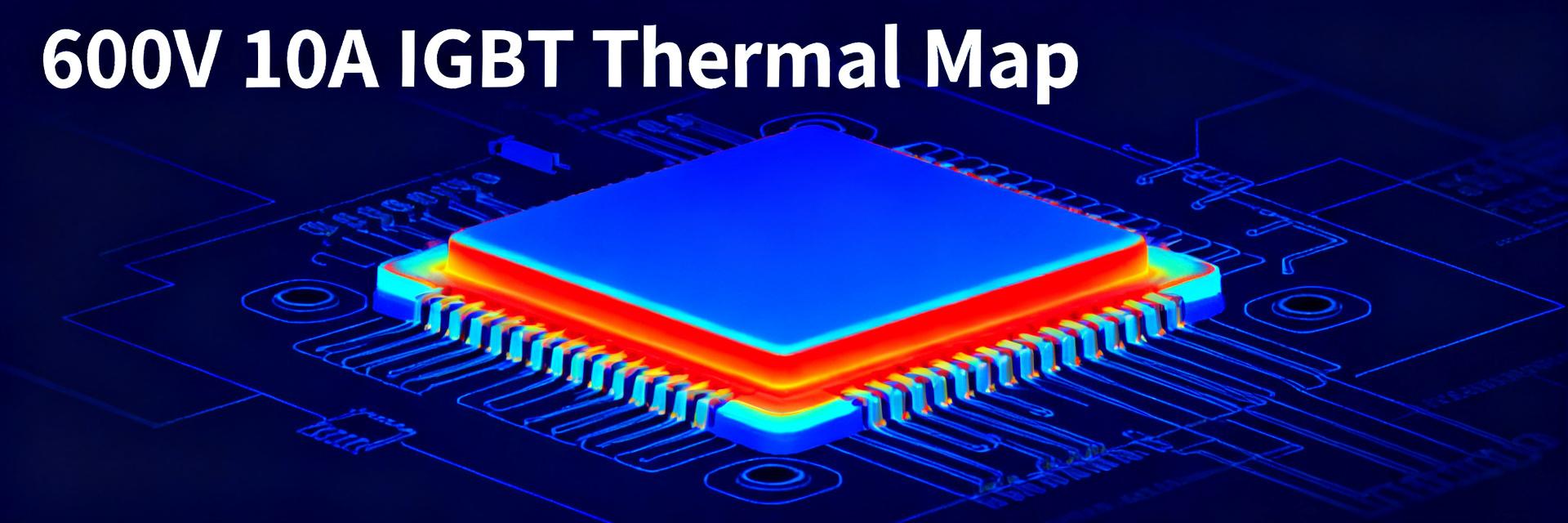
Point: RthJC sets the baseline thermal path; add Rth(heat-sink) and thermal interface to predict Tj. Evidence: Datasheet RthJC values combined with power dissipation yield ΔTj = P·Rth. Explanation: Use ΔTj to size sink and thermal pad; include thermal interface compound RthCS and aim for Tj margin to prevent thermal runaway in sustained high-load scenarios; call out datasheet analysis for thermal figures.
Safe operating area (SOA), short-circuit capability & thermal cycling
Point: SOA and single-pulse short-circuit times limit allowable stress under faults. Evidence: SOA curves show current vs voltage/time limits; short-circuit spec often gives milliseconds of survivability. Explanation: Enforce limits with protection; thermal cycling reduces lifetime—use derating and limit repetitive thermal swing amplitude in power cycling profiles.
Design & selection guide — Using the NGW40T65H3DHPQ IGBT in a real design
Matching device to switching topology (hard vs soft switching)
Point: Suitability depends on switching energy and conduction loss. Evidence: Moderate Eoff/Eon favors soft-switching or resonant topologies but can work in hard-switching with conservative switching frequency. Explanation: For hard-switching, lower frequency or stronger cooling is advisable; in resonant or soft-switch designs, the device’s VCE(sat) advantage improves efficiency and reduces thermal stress.
Gate drive, snubber and protection recommendations
Point: Gate resistor, Miller clamp, and snubber choices control switching stress and EMI. Evidence: Datasheet Qgd and recombination behavior inform resistor selection; Eoff guides snubber energy. Explanation: Start with Rgate mid-range to balance speed and overshoot, use active Miller clamp for aggressive driving, and implement RC or TVS clamping sized for Eoff energy to protect against dv/dt-induced transients—datasheet analysis aids component sizing.
Substitutes, equivalents & sourcing checklist (case-oriented, practical)
How to evaluate equivalents using datasheet parameters
Point: Prioritize electrical and thermal parity when cross-referencing. Evidence: Match VCES, continuous current, VCE(sat), Qg, Eoff, RthJC, SOA, and package pinout. Explanation: Verify dynamic and static behavior under the intended switching conditions rather than just nominal ratings; for NGW40T65H3DHPQ IGBT equivalence, ensure energy and thermal margins align with system limits.
Quick substitution comparison matrix (what to list)
Point: A compact matrix accelerates selection decisions. Evidence: Useful columns include voltage, continuous current, VCE(sat) typ/max, Qg, Eoff, RthJC, package, and recommended derating. Explanation: Populate the matrix with anonymized candidates and run thermal/switching trade calculations to validate substitutes before prototype builds.
| Metric / Spec Parameter | NGW40T65H3DHPQ Value | Equivalent Target | Critical Verification Check |
|---|---|---|---|
| Collector-Emitter Voltage (VCES) | 650 V | ≥ 650 V | Match worst-case transient peak voltages |
| Continuous Current (IC @ 100°C) | 40 A | ≥ 40 A | Check actual package derating curves |
| Saturation Voltage (VCE(sat) Typ) | 1.2 – 1.8 V | ≤ 1.8 V | Keep conduction losses within heatsink limits |
| Total Gate Charge (Qg) | Typical range | ± 15% Max | Ensure peak driver source/sink parity |
| Thermal Resistance (RthJC) | Device optimized | ≤ Original RthJC | Maintain reliability margins under load |
Practical implementation checklist & monitoring recommendations
Pre-production test checklist (bench waveforms and thermal runs)
Point: Bench validation confirms datasheet expectations under real conditions. Evidence: Capture switching waveforms, thermal imaging, short-circuit robustness, and EMI scans. Explanation: Execute tests at target current and frequency, log junction temperature rise, and compare measured Eoff/Eon against datasheet numbers; adjust cooling and gate drive before production.
Field monitoring and failure modes to watch
Point: Monitor telemetry tied to ageing and stress. Evidence: Watch junction temperature margin, collector leakage growth, and gate threshold drift. Explanation: Implement periodic in-system checks and log spikes in leakage or Tj excursions; common failures stem from thermal overstress, SOA violations, or repetitive short events—proactive monitoring prevents field returns.
Summary (conclusion & next steps)
- The NGW40T65H3DHPQ IGBT offers a balanced 650 V / 40 A profile with trench field-stop advantages; designers should prioritize thermal design and SOA margin when committing to switching frequency choices.
- Key trade-offs are conduction versus switching loss—translate VCE(sat) and Eoff/Eon numbers into Pcond and Pswitch, then size heatsink and driver for reliable operation under expected duty cycles.
- Next steps: build a bench test plan, complete a substitution matrix with prioritized parameters, and finalize a gate-drive and snubber strategy to validate system-level loss budgets before production.
Frequently Asked Questions
How do I calculate switching loss from Eoff/Eon for the NGW40T65H3DHPQ IGBT?
Multiply the sum of Eon and Eoff by switching frequency: Pswitch ≈ f × (Eon + Eoff). Add conduction loss Pcond = IC × VCE(sat) (averaged). Verify with measured waveforms since datasheet E values are given under specific test conditions and may differ in-system.
What gate resistor range should I start with given the IGBT specs?
Start with a medium Rgate that yields a driver peak current I ≈ Qg / tr matching your driver capability; typical starting values are tens to low hundreds of ohms depending on Qg and desired dv/dt. Tune for EMI and switching overshoot during bench testing.
Which datasheet parameters are most critical when selecting a substitute?
Prioritize VCES, continuous current rating, VCE(sat) typical/max, total gate charge Qg, Eoff, RthJC, and SOA. Ensure package pinout and thermal path are compatible; validate substitutes under representative switching and thermal conditions before approving for production.
What is the primary operational advantage of the Trench Field-Stop technology in this IGBT?
The trench field-stop architecture reduces the collector-emitter saturation voltage VCE(sat) while minimizing tail current during turn-off, combining low conduction loss with high-efficiency mid-frequency switching.