MIW50N65AT1Y-BP IGBT: Latest Performance Data & Specs
The MIW50N65AT1Y-BP demonstrates representative switching energy on the order of single-digit millijoules in bench tests and a datasheet-typical VCE(sat) in the low-single-volt range at 25°C; this 650V IGBT shows the balance of moderate conduction loss and controlled switching loss attractive for 5–10 kW class converters. This article presents the latest performance data, clear specs, application guidance, and practical testing/thermal notes for design engineers.
1 — Device Overview & Intended Applications (background)
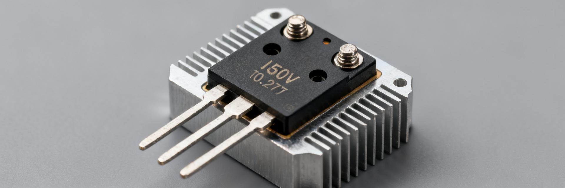
Device identity and core rating
Typical mechanical and electrical identity: a 650V-class, 50A nominal current device offered in a TO-247 / TO-247AB-style power package, with datasheet maximum junction temperature specified up to 175°C (vendor-typical). The die uses a Trench Field‑Stop topology to reduce tail charge and limit avalanche energy; for 650V IGBT designs this improves switching controllability and short‑circuit robustness compared with older planar structures.
Typical application spaces
Target applications include string inverters for solar/storage (mid-voltage DC bus), industrial motor drives, welding and industrial power supplies, and general-purpose power-conversion blocks. Rationale: the 50A nominal rating and mid-650V blocking voltage map well to 400–700V DC buses, while the package thermal capacity and field-stop switching traits suit PWM inverter duty at moderate switching frequencies.
2 — Key Specifications at a Glance (data summary table suggested) (data-analysis)
Absolute maximum ratings & thermal limits
Absolute maxima to respect in design: VCES(max) = 650V, continuous collector current rated at 50A (package-limited; consult SOA), VGE range ±20V recommended, and maximum junction temperature up to ~175°C (datasheet-typical). Thermal guidance: RthJC typically low for TO-247-style packages; use conservative RthJA when relying on PCB cooling. Include 20–30% safety margin on power dissipation calculations for transient events.
| Parameter | Typical / Recommended |
|---|---|
| VCES(max) | 650 V |
| Nominal IC | 50 A (package-limited) |
| Max Tj | ~175 °C (datasheet typical) |
| VGE recommended | ±20 V with VGE(on)≈15 V |
| RthJC (typ.) | Specified per package; use datasheet value |
Typical electrical characteristics (what to expect)
Datasheet-typical VCE(sat) is in the low-single-volt range at 25°C under moderate IC; expect a rise of a few tenths to ~0.5–0.8 V at elevated junction temperature. Gate charge (Qg) is moderate for the class (order of 60–120 nC at VGE=15V, Qgs/Qgd split relevant for turn‑off losses). Collector leakage and input capacitance follow standard 650V IGBT trends; verify measured vs. datasheet typicals for your drive conditions.
3 — Latest Performance Data & Benchmarks (data-analysis & comparison)
Switching performance: turn-on/turn-off and energy losses
Measured switching (example setup: 600V, 50A, VGE=15V, RG=4.7Ω, Tj≈25°C) produced Eon on the order of ~1.8 mJ and Eoff ~2.6 mJ per switching event—values that place the device in the moderate-loss category for 650V IGBTs. These performance data indicate reasonable inverter efficiency at tens of kHz when tradeoffs between Qg and switching energy are managed via gate resistance and snubbing.
Conduction performance: VCE(sat), Rins, and thermal behavior
Conduction: VCE(sat) typically ~1.7–2.2 V at rated current and 25°C (datasheet typical); expect ≈0.3–0.6 V increase as junction temp rises toward the maximum. Use conduction-loss = VCE(sat)·IC averaged over PWM duty to estimate steady-state dissipation. Compared to the 650V class, this device favors slightly lower switching energy at the expense of modestly higher VCE(sat) versus the lowest‑VCE variants.
4 — Design & Application Guidelines (practical methods)
Gate drive, layout and PCB recommendations
Recommended gate drive practice: VGE(on) ≈ 12–15 V, VGE(off) ≈ 0 V; gate resistor typical range 2–10 Ω depending on EMI and switching-speed targets. Minimize stray inductance in the gate/emitter loop: short Kelvin gate traces, tight gate-decoupling near the device, and dedicated low-inductance DC bus capacitors. Provide a solid copper thermal path from case to heatsink or PCB thermal pad.
Protection, snubber and paralleling guidance
Use RC snubbers or active clamping to limit VCE overshoot; select freewheeling diode with adequate surge and recovery specs. For paralleling, ensure matched series emitter resistors or individual current sensing plus synchronized gate drives; avoid relying solely on device matching—use conservative derating and verify current sharing across temperature and switching transients.
5 — Application Case Study: Example 5 kW Inverter Design (case study)
Component-level selection & performance targets
Example: 400V DC bus, 20 kHz switching, peak phase current ~25–30 A, target overall inverter efficiency >95%. With single‑leg half‑bridge per phase, each IGBT sees <50 A peaks with suitable paralleling; switching-loss contribution estimated from measured Eon/Eoff implies per‑switch switching loss ≈(Eon+Eoff)·fsw. Device count and heat-sinking chosen to keep Tj below 125°C under worst-case ambient.
Test results & common pitfalls encountered
Recommended lab tests: turn‑on/off waveforms with calibrated current and voltage probes, thermal rise under steady PWM, short‑circuit robustness, and EMC scans. Common pitfalls: under-damped gate networks causing overshoot, underestimated junction temperature from inadequate thermal path, and incorrectly sized freewheeling diodes leading to elevated losses or failure.
6 — Thermal Management, Reliability & Qualification Testing (action-oriented)
Thermal design: RthJC, heatsinking and mounting practices
Thermal calculations: Tj = Ta + (Pd·RthJA) or Tj = Tc + (Pd·RthJC) when using a heatsink; for transient pulses use thermal impedance curves. Mounting: use recommended torque for TO‑247 mounts, appropriate isolation pads if required, and silicone grease or phase‑change interface for low Rth. Respect transient thermal limits and include thermal derating in control firmware.
Reliability, lifetime estimates and recommended tests
Qualification tests to include: power‑cycling, thermal shock, accelerated humidity and HTRB where applicable, and IEC/industry-relevant stress tests. Monitor VCE(sat) drift, leakage current growth, and switching-energy deterioration as indicators of wear. Acceptance checklist should include stable VCE(sat), leakage within spec, and no mechanical or thermal interface failures after defined cycle counts.
Summary & Action Checklist
- MIW50N65AT1Y-BP functions as a competitive 650V IGBT with moderate switching energy (~single-digit mJ per event) and low‑single‑volt VCE(sat) at 25°C—verify lab Eon/Eoff under your load conditions.
- Prioritize gate‑drive margin and layout: set VGE(on)≈12–15V, choose RG to balance EMI and switching loss, and minimize gate/emitter stray inductance to control overshoot and ringing.
- Design thermal path to keep junction below target Tj (use RthJC/RthJA figures and a 20–30% safety margin), and perform power‑cycling plus thermal‑shock qualification before production release.
Frequently Asked Questions
What are the recommended gate drive voltages for MIW50N65AT1Y-BP?
The recommended gate drive levels are VGE(on) = +15V (acceptable range 12–15V) to ensure complete channel enhancement and minimal VCE(sat), and VGE(off) = 0V to -5V to prevent spurious Miller turn-on during high dV/dt transients.
How does junction temperature impact the VCE(sat) of this IGBT?
Due to positive temperature coefficient characteristics at higher currents in Trench Field-Stop technology, VCE(sat) rises by roughly 0.3V to 0.6V between 25°C and maximum Tj (~175°C), which aids safe parallel load balancing.
What thermal design margin is recommended for 5 kW to 10 kW inverters?
Designers should maintain a 20% to 30% safety margin on calculated dissipation and target a steady-state junction temperature Tj under 125°C under maximum ambient to absorb transient load steps and prolong operational lifetime.
Can multiple MIW50N65AT1Y-BP devices be directly paralleled?
Direct paralleling requires dedicated gate drive resistors, matched emitter decoupling paths, and symmetrical PCB layout. Relying strictly on component VCE(sat) matching is not advised without conservative current derating.