HoFL3-8536-A 25µΩ Shunt Resistor: Full Tech Specs & Limits
Design Insight: For precision current sensing in high-current systems, choosing a low-value shunt with predictable drift is essential. The HoFL3-8536-A-25uR-1% is specified at 25 µΩ with a ±1% tolerance and a 50 W power rating. This combination yields millivolt-level drops at hundreds of amperes while keeping insertion loss small, making it suitable for high-performance battery and power-conversion telemetry.
Application Reality: Practical deployment exposes thermal and mechanical limits not obvious from the nameplate. Continuous dissipation, Temperature Coefficient of Resistance (TCR), mounting pitch, and terminal torque all dictate real-world accuracy. This guide distills measured consequences and integration checks so engineers can validate the component in production designs before field failures occur.
Product Overview: HoFL3-8536-A 25 µΩ Shunt Resistor
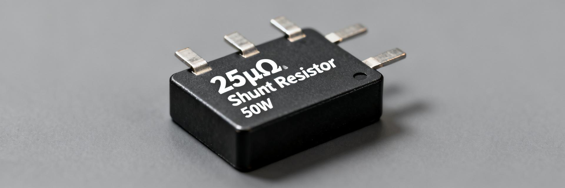
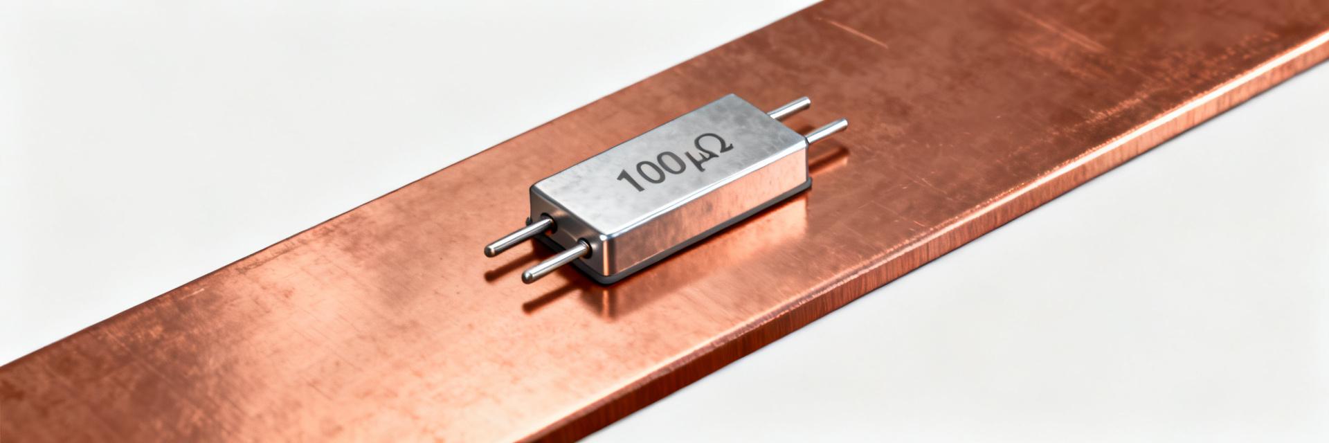
The nominal identity and tolerance set the baseline for system accuracy. The nominal resistance of 25 µΩ at reference temperature and ±1% tolerance define the initial DC offset; a TCR near 150 ppm/°C establishes thermal sensitivity. Engineers must use these three parameters to calculate absolute error at operating currents and to scale instrumentation amplifiers and ADCs accordingly.
Key Specs At-a-Glance
| Parameter | Value |
|---|---|
| Nominal Resistance | 25 µΩ |
| Tolerance | ±1% |
| Power Rating | 50 W (continuous, ref mounting) |
| TCR (Typical) | ≈150 ppm/°C |
| Mounting Pitch | 60 mm |
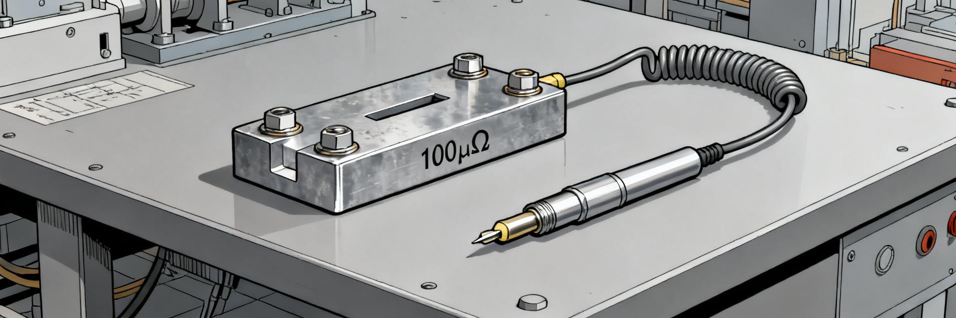
| Footprint | Through-hole with mechanical support |
| Element Material | Manganin/Copper Alloy Power Strip |
Note: Always confirm model marking, tolerance codes, and date/lot fields on incoming components to verify correct revisions.
Electrical Specs Deep-Dive
Resistance, Tolerance, and Temperature Drift
Absolute accuracy is a function of nominal tolerance combined with temperature-induced change. At 100 A, the ideal voltage drop is calculated as:
V = I × R = 100 A × 25 µΩ = 2.5 mV
The ±1% tolerance introduces a ±25 µV offset. A TCR of 150 ppm/°C across a 40°C delta adds 6000 ppm (0.6% deviation), resulting in an additional ~15 µV drop at 100 A. Calculating the total worst-case error budget requires combining initial tolerance, TCR drift, connection/contact variation, and amplifier input offsets.
Power Rating and Continuous vs. Pulse Current Limits
Convert the continuous power rating to maximum allowable current using the power-to-resistance relationship:
I = √(P / R) = √(50 W / 25 µΩ) ≈ 1414 A
While 1414 A is the theoretical thermal limit, practical continuous current is significantly lower due to mounting configurations, surrounding ambient temperatures, and design safety margins. For short current spikes, reference transient pulse energy curves and validate with thermal imaging under full operational load.
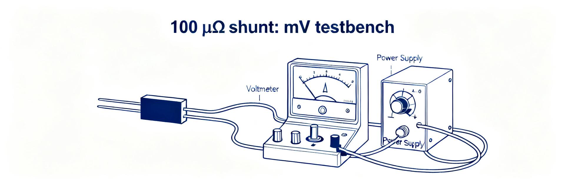
Typical 4-Wire (Kelvin) Connection Topology
Performance Limits & Derating
Thermal Derating & Environmental Boundaries
Continuous power limits decrease dramatically in enclosed spaces or high-temperature zones. When airflow is restricted and heat sinking is minimal, thermal resistance from the shunt element to ambient spikes. A standard industrial design practice is to derate allowable continuous current by 10% to 20% for every 10°C rise above the standard reference temperature. Always model conduction and convection paths to map worst-case scenarios.
Aging, Drift, and Mechanical Stress Limits
Long-term resistance drift is primarily caused by structural thermal cycling and mechanical stress on the terminals. Repeated torque cycles or PCB expansion stress the copper-manganin boundaries, causing minor microstructural changes. Qualify the design through power cycling tests (e.g., 1000 cycles), thermal ramp tests, and terminal torque stability checks to guarantee stability over life.
Measurement & Integration Best Practices
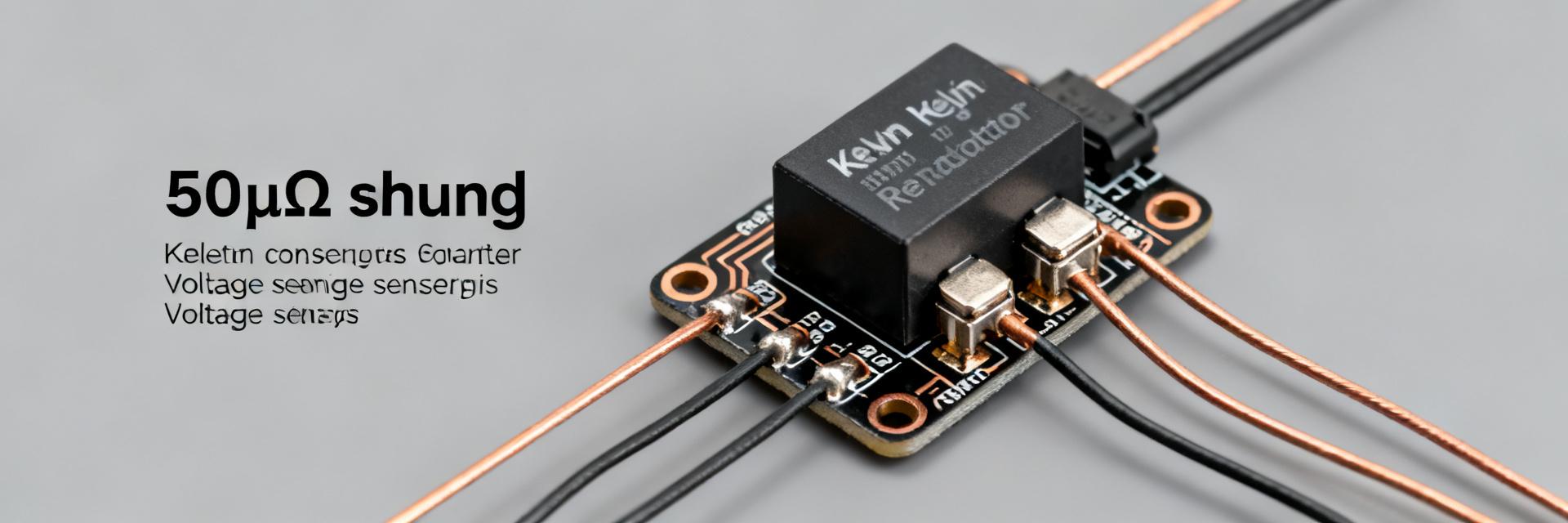
Four-Wire (Kelvin) Sensing Layout
Four-wire sensing is critical to isolate the small micro-ohm voltage drop from high-current conductor losses. At 100 A, a tiny 1 mΩ trace path creates a 100 mV drop, completely masking the 2.5 mV shunt drop. Run independent sense lines directly from the Kelvin terminals to the input amplifier, keep sense traces thin and symmetric, and employ star-grounding principles to eliminate ground loop errors.
Signal Conditioning and Instrumentation Amplifiers
The signal conditioning front-end must resolve millivolt-level signals with minimal noise. For a 2.5 mV drop at 100 A mapping to a 3.3V ADC input, an amplification gain of ~1320 is required. Choose high-CMRR, low-drift zero-drift instrumentation amplifiers, and deploy RC anti-aliasing filters close to the ADC inputs. Implement digital calibration or offset-trimming to compensate for initial system tolerances.
Worked Application Examples
Battery Current Telemetry
In high-peak energy-storage applications, minimizing insertion loss is paramount. A 500 A peak current produces a voltage drop of 12.5 mV and dissipates 6.25 W of thermal energy (P = I²R). Ensure the integration path can dissipate this thermal energy safely and scale the ADC input stage to resolve the required milliampere-level changes.
Inrush & Overcurrent Limiting
Short inrush pulses generate high instantaneous energy peaks. For instance, a 2 ms, 1000 A transient pulse produces an energy spike of:
E = I² × R × t = (1000)² × 25 µΩ × 0.002 s = 50 J
Ensure the shunt's transient thermal capacity is not exceeded and integrate transient voltage clamp diodes to protect sensitive down-stream amplifiers.
Integration Checklist & FAQ
Ensure all items on this checklist are met before moving to production verification: secure mounting, verified Kelvin trace routes, low-drift amplifier selection, digital calibration scheme, thermal-soak testing, and alternative component pathways.