100 µΩ Shunt Resistor Report: Precision Specs & Trade-offs
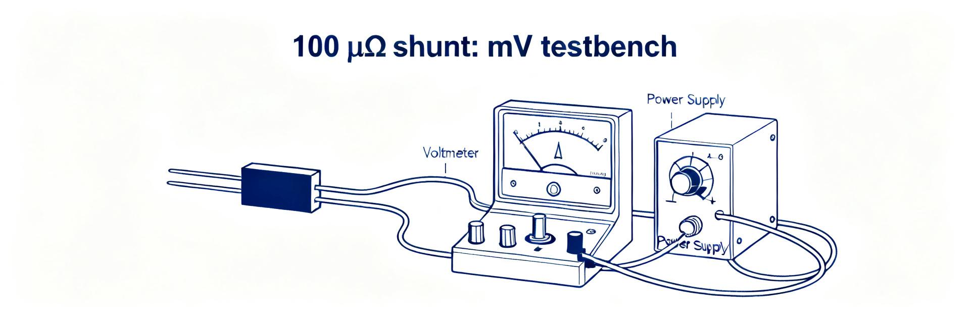
Designers face tightening error budgets in high-current power systems: many EV, datacenter and telecom power stages now require sub-0.1% current measurement accuracy at 50–200 A. A 100 µΩ shunt at 100 A produces a 10 mV drop, so measuring millivolt-level signals reliably demands managing TCR, self-heating and noise. This report on the 100 µΩ shunt resistor delivers data-driven comparisons, measured trade-offs, test methods and a production checklist so engineers can choose and validate a part with confidence for precision current sensing.
Why 100 µΩ shunt resistors matter (background)
1.1 → Typical applications & measurement targets
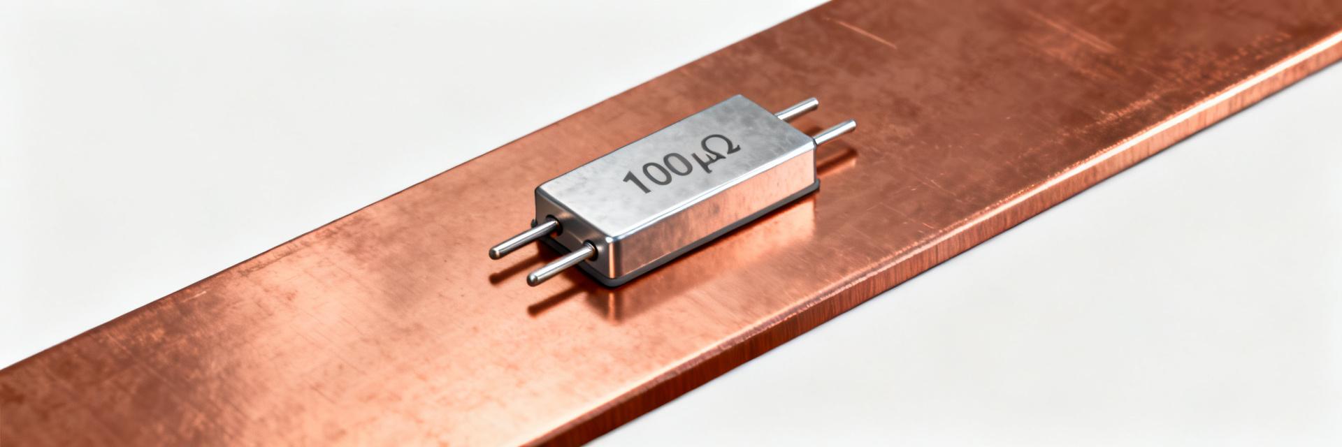
Values near 100 µΩ appear where currents are large and allowable voltage drop is small: high-current battery management, power supplies, motor drives and telecom PSUs. Typical currents span 10–1000 A; common targets are ±0.1% to ±1% accuracy. Voltage-drop examples: 50 A → 5 mV, 200 A → 20 mV. These low drops set amplifier gain, ADC resolution and common-mode requirements for precision current sensing.
1.2 → Basic electrical & thermal constraints designers must accept
Design constraints include low mV signals, I²R heating, thermal gradients across the shunt, TCR contribution to drift and layout parasitics. Quick checklist: limit power loss, set acceptable temperature rise, and provide Kelvin sensing. Mechanical mounting and adequate copper area are equally critical to control thermal gradients that corrupt measurement accuracy.
Quantifying accuracy: TCR, tolerance and self-heating (data analysis)
2.1 → What TCR means for mV‑level measurements
TCR (ppm/°C) converts temperature change into resistance change: ΔR = R·TCR(ppm/°C)·ΔT/1e6. For a 100 µΩ part with 100 ppm/°C and ΔT = 50°C, ΔR = 0.5 µΩ → at 100 A the voltage error is 50 µV on 10 mV (0.5% error). TCR values of 50, 100 and 200 ppm/°C map to progressively larger % errors at 50/100/200 A and must be budgeted explicitly.
2.2 → Modeling self‑heating and transient behavior
Power is P = I²R: 100 µΩ at 200 A dissipates 4 W. Thermal rise depends on thermal resistance to ambient and copper spread; thermal time constants govern transient drift during pulses. Estimate ΔT ≈ P·θth (°C/W) and translate to ΔR via TCR. For pulsed profiles, plot R(t) to capture settling toward steady-state and plan calibration or blanking intervals.
Performance specs & trade-offs for 100 µΩ shunt resistors (data analysis / specs)
3.1 → Voltage drop vs. power loss: practical examples
Worked examples illustrate trade-offs and SNR implications: at 10 A the drop is 1 mV (0.01 W), at 50 A 5 mV (0.25 W), 100 A 10 mV (1 W), 200 A 20 mV (4 W) and 500 A 50 mV (25 W). Higher R boosts amplifier SNR but increases heating and waste; lower R reduces loss but demands lower-noise amplification and ADC resolution.
| Current (A) | Vdrop (mV) | Power (W) |
|---|---|---|
| 10 | 1.0 | 0.01 |
| 50 | 5.0 | 0.25 |
| 100 | 10.0 | 1.00 |
| 200 | 20.0 | 4.00 |
3.2 → Noise, stability, tolerance and long‑term drift
Noise sources include 1/f and Johnson noise; short‑term stability and tolerance classes affect initial accuracy; aging and stress lead to drift. Request datasheet metrics: low‑frequency noise density, short‑term stability under load, and long‑term ppm/year drift. Plan acceptance tests for cycle stability and contact‑induced changes.
Best practices: PCB layout, Kelvin sensing and thermal management (methods guide)
4.1 → Kelvin connection and footprint guidance
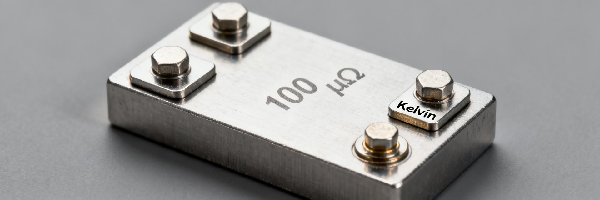
Separate current and sense paths: place Kelvin pads close to the shunt terminals with dedicated thin traces to the amplifier. Keep Kelvin leads short and thermally isolated from heavy current copper. Use multiple vias for current paths and ensure sense vias are separate. A layout checklist should include pad spacing, sense trace routing and mechanical mounting considerations.
4.2 → Thermal paths, heat sinking and mechanical mounting
Provide thermal escape via copper pours, thermal vias and heat spreaders to avoid local hot spots. Ensure sense points are on the same isothermal region as the conductor between current terminals. Use compliant mounting or stress relief to prevent strain that changes resistance under torque or vibration.
Lab test procedures and building an uncertainty budget (methods guide)
5.1 → Low‑resistance four‑wire measurement setups and fixtures
Use true four‑wire kelvin fixtures, a low‑noise DAQ or nanovoltmeter and a stable current source with known stability. Warm up the fixture, perform averaging, and include common‑mode rejection checks. For pulsed measurements, capture time-domain settling; for DC, run long dwell times until thermal equilibrium.
5.2 → Sources of measurement error & how to build an uncertainty budget
Dominant error contributors: source stability, lead/contact resistance, thermal EMFs, instrument noise and TCR during test. Combine contributors via root-sum-square (RSS). A simple uncertainty table should list each term with units in µΩ or ppm and an estimated standard uncertainty for a combined expanded uncertainty.
| Source | Std. Unc. (µΩ) |
|---|---|
| Current source stability | 0.05 |
| Instrument noise | 0.10 |
| Thermal EMF / contacts | 0.08 |
| Combined (RSS) | 0.15 |
Case study: integrating a 100 µΩ shunt in a 48 V / 200 A power module (case study)
6.1 → Design targets, calculations and chosen guardrails
Target: ±0.25% overall accuracy at 200 A. Voltage drop is 20 mV and power 4 W. With a TCR budget of ≤100 ppm/°C and estimated thermal rise of 30°C, expect ~0.3 µΩ shift (~0.15% at 200 A). Amplifier gain and ADC resolution must resolve tens of microvolts to meet the SNR requirement.
6.2 → Test results, PCB changes and final verification checklist
Prototype testing highlights: thermal gradients required copper pour adjustments and relocated Kelvin pads. Final verification includes thermal cycling, long‑duration soak at full current and spot four‑wire checks on production samples. Iterate layout and mounting if drift or hot spots appear.
Actionable checklist: design, testing and procurement (action recommendations)
7.1 → Quick design checklist (on‑board + system‑level)
Numbered checklist: 1) Specify R@20°C, tolerance and TCR curve; 2) define maximum working current and allowable ΔT; 3) include short Kelvin pads and separate sense traces; 4) design copper area and vias for heat spread; 5) plan calibration points and amplifier input conditioning for precision current sensing.
7.2 → Production test & QA checklist
Production tests: inline four‑wire spot checks, batch TCR sampling, thermal cycling and torque/mount integrity checks. Suggested sampling: 1% per lot with full test on first production run. Define pass criteria for resistance, drift after soak and mechanical integrity before shipment.
Summary
Low R keeps power loss low but tightens SNR and amplifier/ADC requirements; TCR and self‑heating are often the largest contributors to error for a 100 µΩ shunt resistor. Use Kelvin sensing, controlled PCB thermal design and explicit TCR budgeting. Run pulsed and steady‑state thermal tests, quantify uncertainty and implement production QA to ensure measurement goals are met in volume production.
Key summary
- Budget TCR early: TCR(ppm/°C) maps directly to percent error at high currents; include it in the uncertainty budget for any 100 µΩ shunt resistor selection.
- Layout matters: short Kelvin leads, separate current and sense paths, and generous copper heat spreading limit gradients that corrupt millivolt measurements.
- Test to verify: four‑wire fixtures, pulsed and steady‑state thermal tests, and a simple RSS uncertainty table provide quantitative acceptance criteria before production.
Frequently asked questions
How much TCR is acceptable for a 100 µΩ shunt resistor?
Acceptable TCR depends on current and accuracy targets; for sub‑0.5% accuracy at 100–200 A, aim for ≤100 ppm/°C. Combine expected thermal rise with TCR to compute ΔR and percent error, and include this term in the overall uncertainty budget before final selection.
What is the recommended Kelvin wiring for a 100 µΩ shunt resistor?
Place Kelvin sense pads immediately adjacent to the shunt terminals on the same PCB plane, route dedicated thin sense traces to the amplifier, and avoid routing sense traces through high‑current copper. Keep sense lead length minimal and thermally isolated from current paths to minimize error from gradients.
How to calibrate out temperature drift for a 100 µΩ shunt resistor?
Measure resistance vs. temperature across the expected operating range to derive a TCR curve, then implement temperature compensation in firmware or hardware. For dynamic systems, use periodic in‑system calibration at known currents or incorporate a temperature sensor near the sense element and correct readings in real time.
Why is a 4-wire (Kelvin) connection mandatory for a 100 µΩ shunt?
Because parasitic contact and lead resistances on a standard 2-wire layout can easily exceed several hundred micro-ohms, completely overriding and corrupting the nominal 100 micro-ohm value. Separate current paths and sense traces ensure the amplifier only measures the true voltage drop across the active element.