MIZ75N65AH2Y-BP Datasheet Deep Dive: Key Specs Explained
The MIZ75N65AH2Y-BP is a 650 V-class IGBT rated for roughly 75 A steady-state operation; selecting a correctly rated IGBT at this class can reduce switching-stage losses by a measurable margin compared with older generations. This article decodes the MIZ75N65AH2Y-BP datasheet and explains the specs engineers need to design reliably, translating key datasheet numbers into thermal, switching, and SOA practices engineers can apply in inverter and motor-drive designs.
1 — What is the MIZ75N65AH2Y-BP? Quick overview and use cases
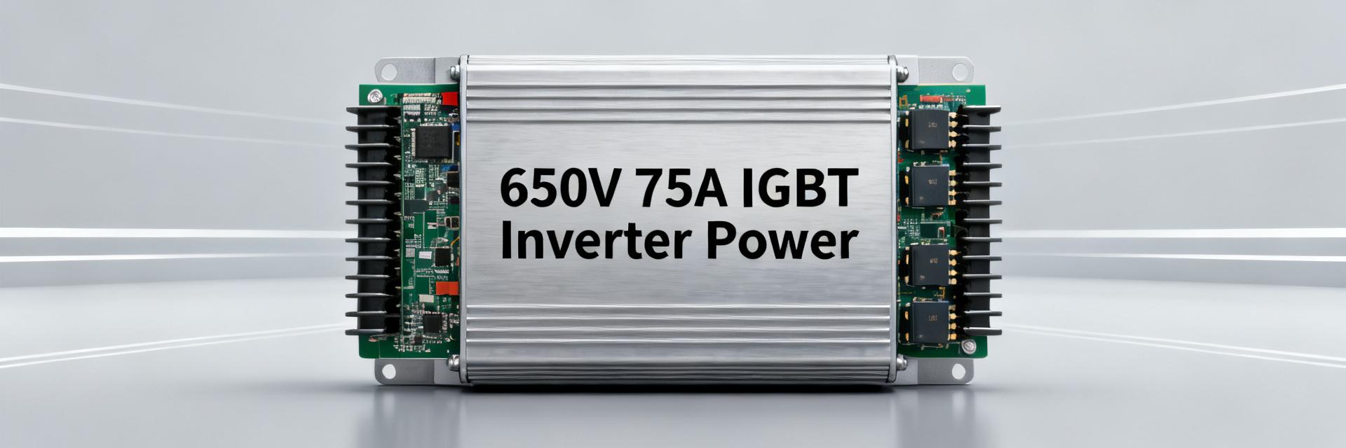
1.1 — Device class, package, and target applications
The MIZ75N65AH2Y-BP is a trench/field-stop IGBT intended for medium-power, high-voltage applications. The datasheet specifies a 650 V blocking rating and a multi-leaded power package (TO-247 compatible multi-lead style). Typical roles include 3-phase inverter half-bridges, industrial motor drives, and switch-mode power supplies where 400–600 V DC buses and pulsed loads are common. A simple half-bridge with RC snubber and a gate-driver isolated power supply makes a clear layout example.
1.2 — Key headline ratings at a glance
Engineers want top-line numbers immediately. The datasheet headline values show nominal Vce rated at 650 V, continuous Ic ~75 A, and a maximum junction temperature around 175°C. Those figures set the envelope for system margining and cooling; listed values should be the first cross-check when selecting this device.
- Nominal Vce (Vces): 650 V
- Continuous collector current (Ic): 75 A
- Max junction temperature (Tjmax): ~175°C
| Key Specification Parameter | Datasheet Rated Value (Headline) |
|---|---|
| Collector-Emitter Voltage (VCES) | 650 V |
| Continuous Collector Current (IC) @ 100°C | 75 A |
| Pulsed Collector Current (IC, pulse) | 225 A |
| Max Junction Temperature (Tjmax) | 175 °C |
2 — Electrical ratings: voltage, current, and safe operating area
2.1 — Breakdown voltage, VCE/VCES, and margin planning
Absolute voltage rating vs recommended operating voltage must be distinguished. With a 650 V Vces, practical designs derate to maintain margin against spikes and dv/dt-induced overshoot. For a 400 V DC bus, a common derating practice is to allow 1.5× margin (400 V × 1.5 = 600 V), leaving limited headroom; for a 600 V bus you need stronger spike-clamping (TVS or RC snubbers) since the margin is small. Example: a 600 V bus with expected 50 V overshoot pushes near Vces limits—add clamping to keep transients <650 V.
2.2 — Continuous current, pulsed current, and SOA limits
Continuous Ic and pulsed/peak ratings are separate items on the datasheet and are governed by the SOA (Safe Operating Area) graph. The datasheet provides pulsed SOA curves and time-limited current ratings. For example, a device rated 75 A continuous may tolerate several hundred amperes for microsecond pulses, but only for short durations and with appropriate thermal mass. Actionable: use the SOA curve to map pulse width and peak current—e.g., a 10 ms pulse allowance can be read directly from the SOA plot to confirm safe switching in burst-mode loads.
3 — Switching characteristics and gate drive implications
3.1 — Gate charge, input capacitance, and drive voltage requirements
Gate parameters (Qg, Qgs, Qgd, Vge(th)) determine driver sizing. The datasheet lists total gate charge and capacitance vs gate voltage. A higher Qg requires a stronger gate driver current to achieve fast edges; typical design balances a gate resistor between 10–100 Ω depending on desired di/dt and EMI. Actionable: select gate resistor 10–33 Ω for faster switching in low-EMI environments, 47–100 Ω where EMI or voltage overshoot is a concern; include a small RC snubber across collector-emitter when dv/dt spikes are observed.
3.2 — Turn-on/turn-off times, Miller effect, and switching loss estimates
Turn-on/off times, combined with Vce×Ic waveforms, give switching-energy estimates. Datasheet switching-energy curves (Eon/Eoff vs Ic and Vce) allow back-of-envelope loss calculations. Approximate switching loss per transition = E_sw (from curve) × switching frequency. Example: if Eon+Eoff ~0.5 mJ per switching event at a given current and frequency is 10 kHz, switching loss ≈ 0.5 mJ × 10k = 5 W per device (assumptions: measured at given Vbus and gate drive). Always verify in-lab with real waveforms; datasheet curves are useful starting points but depend on test conditions.
4 — Thermal, packaging, and reliability parameters
4.1 — Junction temperature, thermal resistance (RthJC/RthJA), and cooling strategy
Thermal stack-up determines allowable dissipation. Typical datasheet entries include RthJC and recommended mounting conditions. Use RthJC to calculate Tj = Ta + Pd × (RthJC + RthCS + RthSA) where Pd is device power loss, RthCS is case-to-sink, and RthSA is sink-to-ambient. Actionable example: for Pd = 20 W and a conservative total thermal resistance of 1.5 °C/W, Tj rise ≈ 30 °C above ambient; design heatsink/cooling to keep Tj below Tjmax under worst-case ambient and transient loads.
4.2 — Ruggedness, short-circuit capability, and lifetime considerations
Short-circuit withstand and ruggedness specs are critical for protection design. The datasheet specifies short-circuit duration limits and thermal cycling guidelines. Many IGBTs tolerate short-circuit for a limited time at specified gate drive conditions; implement fast detection and desaturation protection. Actionable test steps: run prototype short-circuit tests at controlled current, verify thermal runaway thresholds, and perform thermal cycling to validate solder/junction integrity before production.
5 — How to read the MIZ75N65AH2Y-BP datasheet: key figures and graphs
5.1 — Prioritize the graphs: which plots matter most and why
Not all plots are equally relevant; prioritize SOA, Eon/Eoff vs Ic, Vce(sat) vs Ic, and capacitance vs Vce. These curves directly affect thermal, switching, and drive design. Check axes and test conditions—look for ambient temperature, pulse width, and gate drive level. Checklist: 1) confirm test Vbus and gate voltage, 2) read pulse width for SOA points, 3) note measurement ambient, and 4) check if curves are single-point or normalized.
5.2 — Common spec mismatches and questions to verify with vendor/test
Ambiguities often exist in test conditions. Datasheet notes sometimes omit test-fixture thermal path or pulse repetition rate. Verify whether ratings are pulsed or DC, what duty cycle applies, and how junction temperature was measured. Actionable: ask vendor or replicate tests: pulsed SOA at intended pulse width, Rth with your mounting, and switching-energy measurements at your gate-driver settings to confirm real-world behavior.
6 — Application case study + practical design checklist
6.1 — Example: selecting the MIZ75N65AH2Y-BP for a 3-phase inverter leg
Let us walk through component choices for a 650 V-class inverter. Applying bus margin, switching-frequency, and thermal budget from prior sections: for a 400–600 V bus, choose a gate driver capable of ±12–15 V drive. RC snubber values start around R=10–100 Ω and C=100–1,000 pF depending on ringing, and a clamp (TVS or active clamp) to keep transients below Vces. BOM-like companion components: gate driver (15 V, 2–3 A peak), RC snubber (10–100 Ω / 100–1,000 pF), TVS clamp at slightly above bus voltage, adequate heatsink with thermal resistance sized to Pd.
6.2 — Quick action checklist before prototype and production
- Verify headline specs against intended Vbus and derating margins.
- Perform thermal modeling using real Pd and the worst-case ambient temperature limit.
- Bench-test switching energy and SOA parameters at target gate drive specifications.
- Run desaturation and short-circuit protection response tests.
- Complete EMI pre-compliance scanning and thermal cycling validation.
Summary
The MIZ75N65AH2Y-BP provides a balanced 650 V, ~75 A IGBT solution for inverter and motor-drive systems; designers should focus on Vce derating, SOA reading for pulse duty, and thermal path engineering. Key trade-offs are switching speed versus EMI, and gate-driver strength versus dv/dt-induced overshoot—confirm switching-energy and thermal numbers in-lab under your mounting and gating conditions. Use the datasheet as a starting point and validate with targeted prototype tests to ensure reliable operation of the MIZ75N65AH2Y-BP.
Key Summary
- Derate Vce: keep DC bus plus expected transient peaks well below the 650 V rating to avoid overstress.
- Use SOA: read pulse-width-specific SOA curves to size peak currents and duty cycles safely.
- Gate drive matters: balance resistor choice (10–100 Ω) to trade switching loss vs EMI and overshoot.
- Thermal planning: compute Tj from Pd and total Rth chain and validate with prototype thermal measurements.
FAQ
How should I use the MIZ75N65AH2Y-BP datasheet to size my heatsink?
Calculate device power dissipation (conduction + switching losses), then compute Tj = Ta + Pd × total_Rth (RthJC + RthCS + RthSA). Choose a heatsink that keeps Tj below the datasheet Tjmax under worst-case ambient; verify with thermal cycling and in-situ temperature measurements for the final mounting method.
What gate resistor range is recommended for the MIZ75N65AH2Y-BP to balance EMI and losses?
Typical practical ranges are 10–33 Ω for fast switching with controlled ringing in low-EMI contexts, and 47–100 Ω where EMI and overshoot must be reduced. Start with a mid-value (e.g., 47 Ω) and tune on the bench while monitoring Vce overshoot and dV/dt.
How do I interpret the SOA and switching-energy curves in the datasheet?
Confirm each curve’s test conditions (gate voltage, pulse width, ambient) then map your expected current and pulse duration onto the SOA plot. Use Eon/Eoff graphs to estimate switching losses by multiplying energy per transition by switching frequency; always validate with real measurements because test fixtures and temperatures affect results.
What desaturation protection parameters should be set for the MIZ75N65AH2Y-BP?
To protect the MIZ75N65AH2Y-BP during short-circuit faults, configure a desaturation protection circuit (DESAT) with a threshold voltage typically set around 6.5V to 7.0V. The blanking time must be tuned between 2µs to 3µs to prevent false triggering during turn-on transients while ensuring safe shutdown.