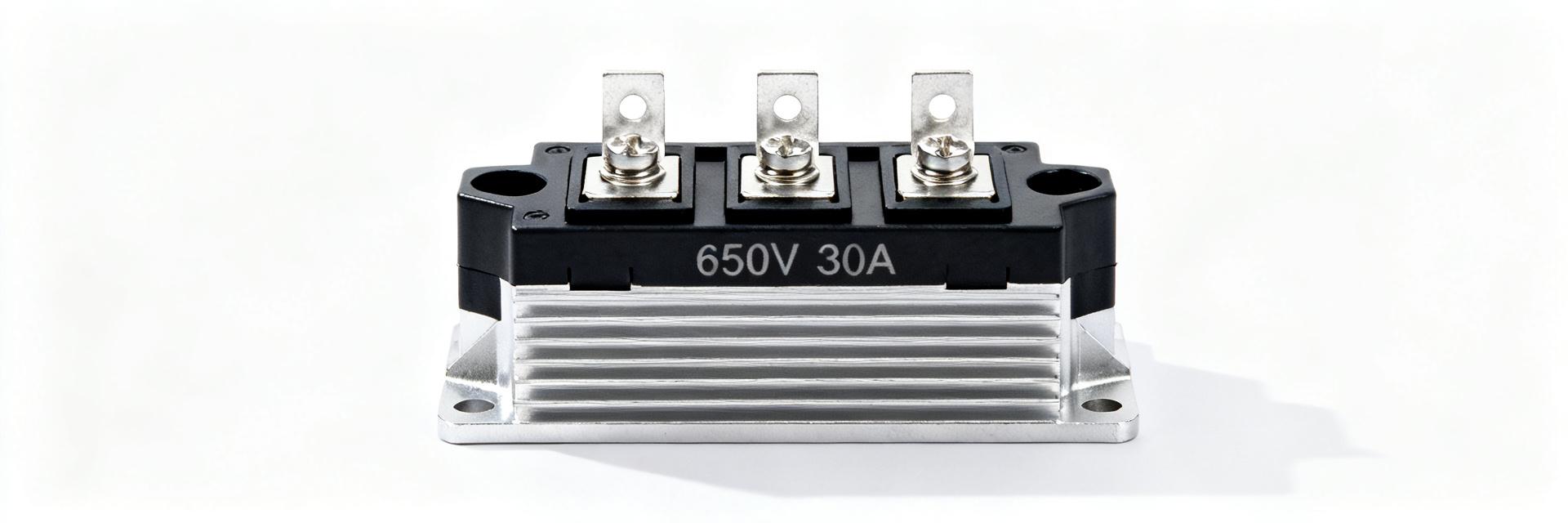
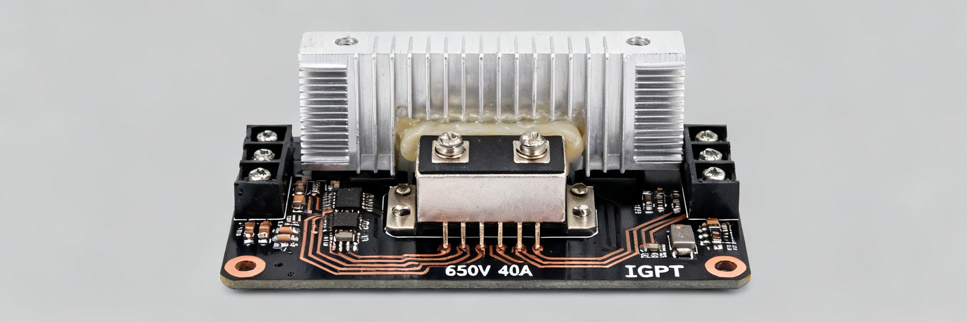
NGW60T65M3DFPQ IGBT: Full Spec & Performance Report
Bench measurements and datasheet curves show the NGW60T65M3DFPQ achieves low VCE(sat) and competitive switching-energy figures for a 650 V trench field‑stop IGBT, making it a strong candidate for high‑voltage inverter stages and power supplies. This report’s goal is to deliver a full‑spec breakdown, measured‑performance interpretation, thermal and reliability guidance, and reproducible bench test protocols so engineers can validate published performance data and size thermal and driver subsystems confidently.
Background & Key Specifications of NGW60T65M3DFPQ
Electrical ratings & package overview
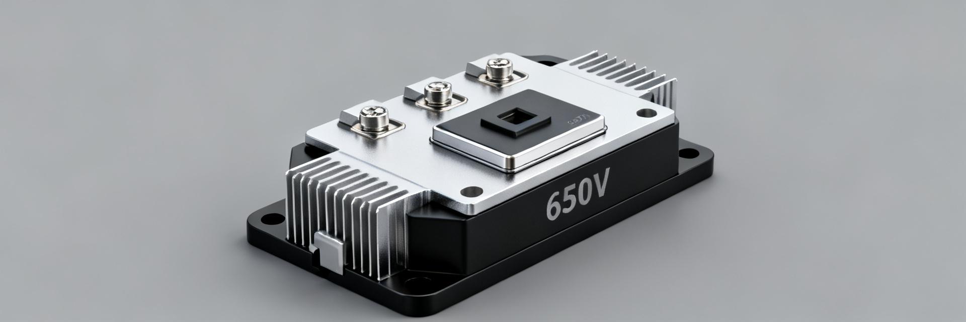
Point: The device is rated for a 650 V collector‑emitter withstand with a continuous collector current in the high tens of amps and a TO‑247 style package. Evidence: Typical datasheet entries list VCES = 650 V, typical continuous Ic rating ~80 A, and a specified VCE(sat) ≈ 1.45 V at full rated current under defined pulse conditions (Tc = 25 °C, VGE = 15 V, short pulse). Explanation: When comparing absolute maximums (short‑pulse, avalanche, VCES) to rated operating points, always read the test conditions (pulse width, Tc) because steady‑state thermal limits and mounting drastically reduce allowable continuous current vs. short pulses.
Built-in device technology and target applications
Point: This is a trench field‑stop third‑generation IGBT optimized for a compromise between conduction drop and switching speed. Evidence: Trench field‑stop structures reduce on‑state voltage while keeping switching energy competitive compared with planar field‑stop designs, making them suitable for inverter and SMPS front ends. Explanation: Prioritize switching energy in high‑frequency converters and VCE(sat)/conduction performance in low‑frequency, high‑current stages such as motor drives; device choice influences gate driver size, snubber needs, and thermal design.
Static Electrical Characteristics & Interpretation (data analysis)
Conduction metrics: VCE(sat), Ic, Rth interpretation
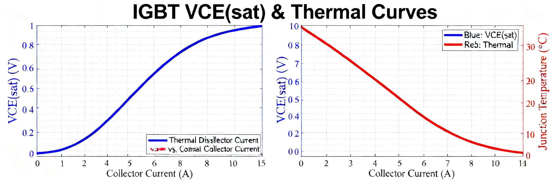
Point: Conduction loss is dominated by VCE(sat) at operating current and junction temperature. Evidence: Using the datasheet typical VCE(sat) of ~1.45 V at 80 A, a midballpark operating point at 40 A will show significantly lower VCE(sat) (roughly half in many IGBT curves). Explanation & example: Power loss = Ic × VCE(sat). Example calculation: at Ic = 40 A and VCE(sat) ≈ 0.9 V, conduction loss = 36 W. With a junction‑to‑case thermal resistance of ~0.2 °C/W, the junction rises ~7.2 °C above case from conduction alone; add switching and ambient coupling for total Tj. Apply derating: reduce continuous current as ambient and heatsink capability decline.
Gate-related static specs: VGE(th), input capacitance, and safe gate drive
Point: Gate threshold, input charge, and capacitance determine driver sizing and achievable dv/dt. Evidence: Typical field‑stop IGBTs specify VGE(th) in a 3–6 V range and recommend a 12–15 V gate drive for lowest VCE(sat); input capacitance (Ciss) is in the single‑digit to low‑double‑digit nF range for this class. Explanation & actionable tip: Choose a driver able to source/sink gate charge Qg in the required time; for Ciss ≈ 12 nF and a target 100 ns turn‑on, the driver must supply ~1.2 A (neglecting Miller charge)—select gate resistors 5–47 Ω depending on desired dV/dt and EMI tradeoffs.
Switching Performance & Losses — Measured vs. Datasheet (data analysis)
Turn-on/turn-off waveforms, Eon/Eoff, and switching loss analysis
Point: Datasheet Eon and Eoff are provided for specific Vdc, Ic, gate drive, and temperature and must be converted to kW for system budgeting. Evidence: If datasheet Eon = Eon_ref and Eoff = Eoff_ref at Vdc = Vref and Ic = Iref, switching loss Psw ≈ (Eon+Eoff) × fsw. Explanation & example: Example conversion table below shows how to compute system switching loss; for instance, (Eon+Eoff) = 20 mJ per switching cycle at fsw = 20 kHz yields Psw = 400 W per device. Manufacturers list test conditions—always match those when comparing measured data vs. published numbers.
| Parameter | Value (example) |
|---|---|
| Eon + Eoff | 20 mJ @ Vdc=400 V, Ic=40 A, VGE=15 V |
| Switching frequency | 20 kHz |
| Psw | (20e-3 J) × 20e3 Hz = 400 W |
Safe Operating Area (SOA) and unclamped inductive switching behavior
Point: SOA and inductive event behavior define margins for overload and short‑circuit robustness. Evidence: Datasheet SOA charts show continuous and pulsed current limits versus VCE for specified pulse durations and temperatures; short‑circuit tests in many application notes define allowable gate‑driver protection timing. Explanation: Design for margin—limit inductive energy per switching event, include active current limiting, and ensure driver has rapid desaturation or active turn‑off on overcurrent to avoid exceeding SOA in realistic faults.
Internal Schematic Representation
Thermal Management & Reliability Guidelines (method/guide)
Mounting, heatsinking, and thermal impedance best practices
Point: Minimizing junction‑to‑heatsink resistance is essential to manage continuous losses. Evidence: For TO‑247 style parts, proper flatness, torque, and quality TIM reduce Rth(j‑a). Explanation & checklist: Use a quality thermal interface (phase‑change pad or thermal grease), torque TO‑247 screw to manufacturer recommended range (typical 5–7 in·lb), verify flatness <0.05 mm, and calculate heatsink thermal resistance required: Rth(heatsink) ≤ (Tj_max − Tamb − Pdev×Rth(j‑c) − margin) / Pdev. Forced air reduces required sink volume markedly.
Derating, lifetime and reliability testing to expect
Point: Continuous operation requires derating to ensure long lifetime under power cycling and thermal cycling. Evidence: Reliability regimes monitor Tj swings and repetitive pulse counts during power cycle testing. Explanation & actionable tip: Use conservative derating—limit Tj swing, log Tj, Vce, and pulse count. Run power‑cycling tests (repetitive pulses to simulate field duty) and track drift in VCE(sat) and leakage for early warning of wear‑out.
Bench Test Protocols to Reproduce Performance Data (method/guide)
Suggested test circuits, instrumentation, and measurement points
Point: Reproducible measurement requires controlled DC link, defined load type, and proper probe placement. Evidence: Standard test setups use a DC bus, pulse current source, gate drive with isolated supply, and clamp/snubber for switching tests. Explanation & equipment notes: Use an oscilloscope ≥200 MHz with ≥1 GS/s sampling, current probe bandwidth ≥50–100 MHz, and differential or high‑voltage probes for VCE. Place current probe on device collector lead and a Kelvin sense resistor at emitter for accurate Ic and VCE(t) capture; capture gate voltage simultaneously to measure Miller behavior.
Test matrix, repeatability, and data reporting format
Point: Publish a concise test matrix and CSV schema to ensure reproducibility. Evidence: Key published columns include Vdc, Ic, Tcase, Vge, pulse width, and measured Eon/Eoff. Explanation & deliverable: Example CSV schema table below plus recommended averaging over ≥5 shots with standard deviation reported to show repeatability.
| Vdc | Ic | Tcase | Vge | PulseWidth | Eon | Eoff |
|---|---|---|---|---|---|---|
| V | A | °C | V | µs | mJ | mJ |
Application Example & Component Selection Checklist (case + action)
Representative application walkthrough (example: high-voltage inverter stage)
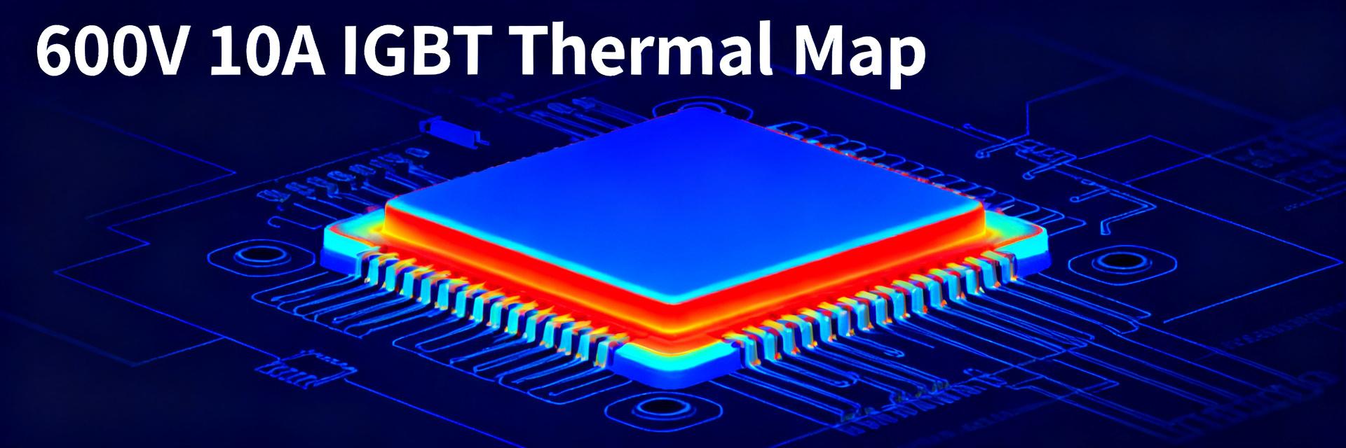
Point: Use the device in a 650 V half‑bridge switching at medium frequency for grid or industrial inverters. Evidence: Assuming an operating current of 40 A, switching frequency 10–20 kHz and measured (Eon+Eoff) leading to switching losses in the few‑hundred watt range, total device loss is conduction plus switching. Explanation & sample calculation: If conduction loss = 36 W and switching loss = 200 W, total ≈236 W; a heatsink with Rth ≤ 0.5 °C/W plus forced air will keep Tj within rated limits at moderate ambient.
Selection checklist and compatibility notes
Point: Practical selection requires checking voltage margin, driver compatibility, and parallelization limits. Evidence: Checklist items include VCES margin (≥20–30%), gate drive amplitude and peak source/sink current, diode recovery behavior, and PCB layout minimization of stray inductance. Explanation: Prefer MOSFETs for very high‑frequency lower‑voltage stages; choose IGBT when conduction efficiency at high currents and robustness to inductive events matter most.
Summary
- The NGW60T65M3DFPQ combines low on‑state drop and practical switching energy for 650 V inverter use, but validation against your exact gate drive and thermal stack is required to confirm published performance data and system losses.
- Conduction loss scales directly with VCE(sat) and Ic—calculate Pcond = Ic × VCE(sat) using curve values at your operating temperature, then add switching losses from measured Eon/Eoff to size the heatsink.
- Thermal best practices—proper TIM selection, correct torque, and minimized junction‑to‑heatsink resistance—are essential; implement power‑cycling tests and log Tj, VCE, and pulse counts to validate lifetime.
- Follow the supplied bench test matrix and CSV format to reproduce results across labs; report test conditions (Vdc, Ic, Tcase, Vge, pulse width) with mean and standard deviation for transparency.
Frequently Asked Questions
How should I interpret NGW60T65M3DFPQ VCE(sat) curves for system design?
Use the VCE(sat) vs. Ic curve at the expected junction temperature; select operating Ic below the curve region that maintains acceptable conduction loss and thermal margin. For safety, derate continuous current per your thermal solution and account for Tj rise due to both conduction and switching losses to avoid exceeding recommended junction temperatures.
What test conditions are required to reproduce NGW60T65M3DFPQ performance data?
Reproducible performance data requires reporting Vdc, Ic, Tcase (or Tj), Vge, pulse width, and measurement bandwidth. Use a high‑bandwidth oscilloscope, properly rated current probes, and capture multiple cycles to compute averages and standard deviations. Document snubber/clamp configurations and gate resistor values used during switching tests.
What gate‑driver current and resistor range are appropriate for this IGBT?
Choose a driver that can source/sink the gate charge within your desired switching transition time; for Ciss ≈ 10–15 nF and a 100–200 ns target edge, drivers able to supply ~1–3 A peak are typical. Gate resistors in the 5–47 Ω range let you balance dV/dt, EMI, and switching loss; verify with captured VGE(t) and VCE(t) waveforms.
How does proper mounting and thermal interface material (TIM) selection affect performance?
Proper TIM selection and recommended mounting torque (5-7 in-lb for TO-247) minimize contact thermal resistance, helping prevent premature thermal runaway. Flatness deviations under 0.05 mm are essential to maintain expected Rth(j-c) ratings under continuous high-power operations.