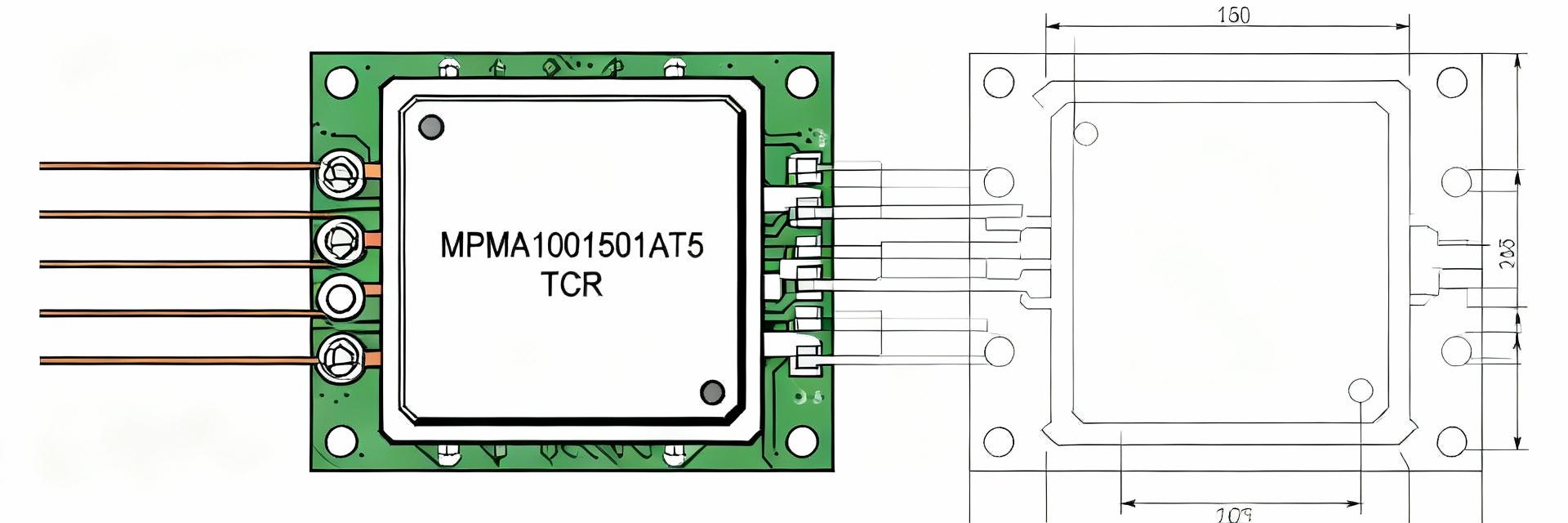
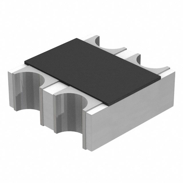
Measured and datasheet values for the MDP1603100KGD04 show a 250 mW power-per-element rating, ±100 ppm/°C TCR, and an operating window from −55°C to +125°C. These parameters define its usable thermal limits and derating strategy.
Product Overview — MDP1603100KGD04 at a Glance
Key Nominal Specifications
| Parameter | Value / Description |
|---|---|
| Element Count | Multiple-element array (refer to datasheet) |
| Package / Pin Count | Chip-array package, multi-lead |
| Resistance Value(s) | Application-dependent; select per design requirements |
| Power per Element | 250 mW (Continuous, Ambient-limited) |
| TCR | ±100 ppm/°C |
| Rated Operating Temp | −55°C to +125°C |
| Typical Tolerance | Datasheet typical tolerances; use matching specs for networked use |
| Mounting / Footprint | SMD footprint; PCB copper and via strategy affect thermal path |
Summary Point: The table lists the critical specs designers must parse. Power-per-element and TCR are explicit datasheet numbers. These are absolute electrical ratings; typical tolerance and matching are performance statistics that should be validated in production sampling before use in precision circuits.
Typical Applications & Constraints
This device is suited for precision resistor arrays, matched networks, and low-power signal paths. With a 250 mW rating per element and ±100 ppm/°C TCR, it is ideal for precision voltage dividers, sensor signal conditioning, and matched attenuators.
✔ Recommended Use
- ● Precision voltage dividers
- ● Sensor signal conditioning
- ● Matched attenuators
✘ Critical Constraints
Avoid power-distribution roles or high-current shunt applications where single-element dissipation exceeds the 250 mW limit. Not ideal for power-sharing without distribution across elements.
Electrical Performance & Tolerance Analysis
Resistance Tolerance & Power Handling
Tolerance and matching directly affect system error budgets. The 250 mW rating sets voltage and current ceilings per element.
Example Calculation: Max Voltage (Vmax = √P·R)
Note: Values based on 250 mW limit.
Temperature Coefficient (TCR) & Drift
The MDP1603100KGD04 TCR performance (±100 ppm/°C) determines short-term and range drift. Over a −40°C to +85°C span (ΔT = 125°C), a ±100 ppm/°C drift yields a resistance change of ±1.25%. In matched arrays, common-mode drift can cancel, but mismatch in elements multiplies error.
Thermal Behavior & Derating (Data-Driven)
Operating Temperature Range
Rated range is −55°C to +125°C, but usable dissipation falls with rising ambient temperature. Conservative guidelines suggest:
Thermal Path Considerations
- Maximize thermal vias under pads.
- Connect to internal or top copper pours.
- Isolate heat-sensitive neighboring elements.
- Use staggered thermal via patterns.
Test Methodology & Qualification
Recommended Test Setup & Procedures +
Repeatable setup is essential. Document FR4 thickness, copper area per pad, and instruments (precision 4-wire DMM, thermocouples, thermal camera). Record element leads and substrate temperature over a 5–15 minute period to reach steady-state.
Stress Tests: Power Soak & Thermal Cycling +
Ramp element power in 10–20% steps holding to steady-state; thermal cycle −55°C to +125°C with 15–30 min dwell for multiple cycles. Perform long-duration soak at 85°C for endurance validation.
Common Failure Signatures & Troubleshooting +
Look for drift beyond tolerance, opens, or delamination. Root causes often include overpower, inadequate thermal paths, or mechanical assembly stress. Use thermal scans to reveal hotspots compared to expected profiles.
Design Guidance — Integration Best Practices
Derating Rules
Operate at 50–70% of rated power at high ambient (above 70°C). Apply an additional 10–20% margin for long-term reliability in critical paths.
PCB Layout Tips
Use enlarged pads with thermal relief. Control solder volume to avoid tombstoning. Place high-heat sources apart to minimize thermal coupling.
Validation
Perform post-reflow resistance checks to detect assembly-induced shifts and validate with thermal imaging during full-load operation.


