-
- 联系我们
- 隐私政策
- 条款 和 条件
- Cookies 政策

4310R-101-104阻网络:完整的规格和测试的数据
数据手册和实验台测量显示,4310R-101-104是一个9电阻、10针母线SIP电阻网络,标称元件为100 kΩ,容差2%,TCR±100 ppm/°C,总耗散约1.25瓦——非常适合紧凑的上拉/下拉阵列和匹配偏置网络。本文提供完整的规格、可重复的测试方法、具代表性的测量结果以及工程验证的实用设计/替代指导。
产品背景与核心规格(背景介绍)
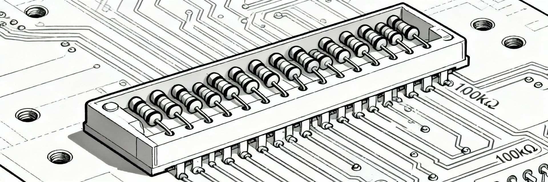
主要电气规格
标称电阻:每个元件100 kΩ;公差:2%(标准)。元件:总线SIP中的9个电阻,总引脚:10。TCR指定为±100 ppm/°C(厚膜规格,在定义的温度间隔内测量)。功率:每个元件≤200 mW(按温度降额),总网络耗散≤1.25 W。工作温度范围通常为−55°C至+125°C。使用下面的规格表进行紧凑参考,并在生产前验证特定批次数据。
| 参数 | 值 |
|---|---|
| 配置 | 9× resistors, bussed SIP (10 pins) |
| 电阻(标称) | 100 kΩ |
| 宽容 | ±2% |
| TCR | ±100 ppm/°C |
| 每元素功率 | ≤200 mW |
| 总耗散 | ≈1.25 W |
| 工作温度 | −55 °C 至 +125 °C |
| 包装 | 模塑SIP,总线连接;符合RoHS标准 |
机械和引脚要领
引脚编号:10个引脚,中心公共(总线)加上9个单独的电阻器引脚。通孔SIP的典型主体长度很紧凑——请查看数据表以了解确切的占地面积和公差。处理:通孔引线接受标准焊角;在波峰焊过程中避免过多的回流热。下面是一个简单的ASCII引脚图,说明了PCB的总线/常见布置,以供参考。
Pin1 Pin2 Pin3 Pin4 Pin5
o-----o-----o-----o-----o测试台方法与测量电气性能(数据分析)

  测试设置和测量程序
  推荐设备:4½位万用表、LCR表、恒温箱、稳压直流电源、数据记录仪和强制空气进行热测试。在三个环境点(例如,25°C、85°C、-40°C)进行测量,每个点浸泡5-10分钟。对于TCR使用电阻随温度扫描;对于功率降额,对每个元件逐级增加电压/电流,同时监测温度上升和电阻变化。使用n≥10个单元进行基本统计置信度。

  测量结果与解释
  报告平均阻力、标准偏差、最小/最大范围和相对于温度和功率的百分比变化。示例样本表格(代表性):
| 公制 | 测量 |
|---|---|
| 平均R(25°C) | 100.2 kΩ |
| 标准差(n=10) | 0.9 kΩ (≈0.9%) |
| TCR(斜率) | ≈+95 ppm/°C |
| ΔR @ 200 mW elem | +0.6% after 30 s |
解释:总线元素之间的比率稳定性通常比绝对漂移更好;当相邻电阻耗散功率时,注意开路元素和热相互作用。绘制电阻与温度的关系以及%变化与施加功率的关系,以获得清晰的通过/失败标准。
应用与设计注意事项(方法指南)
Where to use this resistor network
常见用途:用于多IO总线的上拉/下拉电阻,用于参考和偏置网络的匹配阵列,以及用于逻辑线的无源电阻总成。相比分立元件的优势包括节省电路板空间、匹配的热行为和减少组装时间。示例电路:(1) MCU IO总线上拉阵列,(2) 8通道分压器为多输入比较器提供共享公共节点。
尺寸、降额和PCB布局提示
计算元件功率: P=每个电阻器的V²/R。根据数据表,线性降低70°C以上的功率,以保持每个元件低于200毫瓦。保持引线周围的PCB铜以进行热扩散,在SIP下谨慎使用热通孔,并在大功率相邻电阻器之间留有间隙以减少热耦合。清单:验证每个元件的功率、倒铜量、通孔位置和焊点尺寸。
替换和兼容性清单(案例研究风格)
何时选择替代或升级
如果需要更严格的容忍度,请考虑替换(
Spec matching checklist for safe substitution
Printable checklist: match resistance value per element, tolerance, TCR, number of resistors/pinout, power per element and total, package footprint and environmental ratings (temp/humidity). Verify mechanical fit, derating curves and expected ratio stability before committing to a cross.
Custom styled list to control marker appearance (adjusted ::marker equivalent)- Resistance and tolerance match
- TCR and derating behavior
- 引脚和封装兼容性
- 每个元件的功率和总耗散
- 环境和焊接等级
实用测试清单和样品实验室报告(行动建议)
逐步测试清单
1) Visual and continuity inspection; 2) Initial cold resistance at 25°C for all elements; 3) TCR sweep (−40 → +85°C or wider) with soak and record; 4) Power/thermal test: apply stepwise power to single element up to derated limit; 5) Post‑stress resistance check and humidity/aging if required. Include ESD and safety precautions when handling and powering networks.
Sample lab report template & recommended data presentation
Report sections: Summary, Equipment, Test Conditions, Raw Data, Plots (resistance histogram, R vs T, %Δ vs power), Pass/Fail and Recommendations. Example conclusion language: “Units conform to datasheet specs for resistance, TCR and power derating under tested conditions; no open elements or unacceptable drift observed.”
Key summary
- The 4310R-101-104 is a compact 9‑resistor, 10‑pin bussed SIP resistor network with 100 kΩ elements and 2% tolerance; validate per‑element power and TCR during qualification.
- 台架测试应包括电阻分布、TCR扫描和功率降额,n≥10个单位;将结果显示为平均值/标准差、R vs T和%变化vs功率图。
- 使用替代检查表匹配电阻、公差、TCR、引脚和功率;注意热耦合和PCB铜以确保可靠运行。
常见问题
手风琴常见问题解答,使用细节/摘要(原生、语义、有利于SEO)如何在我的实验室中验证4310R-101-104 TCR?
What are typical failure modes for this resistor network?
Can I use the 4310R-101-104 for high‑voltage applications?
-
 ULH 120 750 J FL=500 功率电阻器:数据手册深入解析2026-05-19 10:07:44 0面向电力电子设计师和工程师的专业技术分析。 额定连续功率 120 W,脉冲能量 750 J,配备 FL=500 引线 —— 这在实践中意味着什么?本数据手册深度解析将这些核心指标转化为电力电子领域的选型、安装和测试建议。建议阅读时间:约 6–8 分钟。 目标受众:必须安全地进行高能线绕电阻尺寸选择、验证和部署的电力电子设计师、测试工程师和采购专业人员。本文旨在通过对数据手册逐行、侧重应用的解读,使工程师能够充满信心地进行操作。 1 — 快速概览与核心规格(背景介绍) 重点关注的关键电气额定值 要点: 首先提取核心电气额定值,以便快速筛选候选器件。证据: 标称连续功率 120 W;脉冲能量额定值 750 J;电阻公差示例 J = 5%;引线样式由代码 FL=500 表示(500 mm 引线)。说明: 这三个指标(连续功率、脉冲能量和引线样式)决定了该组件是否满足子系统的热力、瞬态和机械约束。 参数 典型值 / 备注 连续功率 120 W(参考环境温度下) 脉冲能量 750 J(单次脉冲安全能量) 阻值与公差 按代码范围;公差 J = 5% 引线样式 FL=500 → 引线,500 mm 封装 金属外壳线绕式 机械外形与连接器 要点: 该封装为带长引线的金属外壳线绕电阻。证据: FL=500 表示 500 mm 绝缘引线,适用于远程安装。说明: 利用引线将电阻放置在远离敏感组件的位置或连接至母排;核对数据手册尺寸图中的安装孔位置和间隙,确保热路径和应力释放正确。尺寸图建议替代文本:“ULH 120 750 J FL=500 尺寸图”。 2 — 电气性能深度解析:连续、脉冲与过载行为(数据分析) 连续功率、降额与环境依赖性 要点: 连续额定值必须根据环境温度和安装方式进行降额。证据: 数据手册参考温度(通常为 40°C)下的额定功率为 120 W。说明: 如果数据手册提供了线性降额曲线,请查阅功率 vs. 环境曲线;如果没有,请应用保守的降额规则。计算示例: 假设超过 40°C 后每摄氏度降额 1%,在 60°C 环境下,允许功率 ≈ 120 W × (1 − 0.20) = 96 W。行动: 参考数据手册降额曲线,在无法获得制造商曲线时使用保守示例。 脉冲能量、浪涌承受能力与安全工作区 要点: 脉冲能量 (750 J) 决定了单次事件的温升和安全重复率。证据: 数据手册脉冲额定值通常规定了每次脉冲的能量和建议的重复限制。说明: 通过假设热点的热质量和比热容,将脉冲能量转化为温升。计算实例: 假设热质量 m = 0.05 kg,c = 450 J/kg·K → ΔT ≈ 750 J / (0.05×450) ≈ 33°C。预留 20–30% 的安全裕度:按每次脉冲升温 ≤25°C 设计,并根据手册重复指南留出冷却间隔。 3 — 热管理、安装与降额实践(方法指南 / 数据分析) 热阻、散热与安装最佳实践 要点: 最小化从热点到环境的热阻以维持连续功率。证据: 数据手册可能列出 Rth 或提供功率 vs. 温度曲线;如果没有,请使用测得的降额进行估算。说明: 建议的安装方式:平整、清洁的金属表面;如果允许,使用薄的高导热界面材料;将螺钉拧至规定范围,并使用星形垫圈确保电气和机械安全。下方的安装清单可确保可重复性。 表面平整度:接触区域内 ≤0.1 mm。 导热化合物:如果需要,使用薄的电绝缘层。 螺钉扭矩:遵循数据手册 —— M4 紧固件通常为 1.5–2.5 N·m(请验证部件图纸)。 隔离:需要电气隔离时,使用云母片或导热垫。 环境限制与可靠性考量 要点: 如果处理不当,环境压力会缩短寿命。证据: 数据手册列出了工作温度、湿度和振动限制。说明: 对于恶劣环境,应用额外的降额(例如减少 10–30% 的功率),并强制执行部署前的热循环和振动验收测试。跟踪腐蚀、引线疲劳和绝缘击穿等故障。 4 — 应用场景与选型清单(案例聚焦 + 方法) 典型用例及为何该电阻适用 要点: 使电阻规格与应用的能量/时间曲线相匹配。证据: 常见应用包括动态制动、负载箱、浪涌限制和测试台,这些场合需要高单脉冲能量和中等连续耗散。说明: 对于动态制动,优先考虑脉冲能量和峰值电压;对于连续负载箱,优先考虑稳态功率和散热。在对应应用时,对脉冲能量和连续功率使用安全裕度 (20–30%)。 替代规则与等效选型指南 要点: 了解在进行替代时哪些参数是不可妥协的。证据: 脉冲能量、峰值电压和引线样式通常不能妥协。说明: 公差或物理尺寸有时可以权衡;如有疑问,请选择更高脉冲能量和至少相等的连续功率,或者并联多个电阻以确保电流均分,并考虑增加的 ESR 和电感影响。采购清单: 所需功率和脉冲、引线长度 FL=500、间隙以及所需的认证。 5 — 安装、验证测试与维护清单(行动建议) 预安装和台架验证测试 要点: 在集成前验证收到的每个单元。证据: 数据手册测试建议通常包括绝缘电阻和电阻公差测量。说明: 标准检查:外观检查、兆欧表绝缘测试(如果适用)、受控温度下的直流电阻测量,以及在用热电偶监测金属外壳温度并用示波器验证脉冲波形的同时,进行一两次低能脉冲测试。通过/失败标准: 电阻在公差范围内;每次脉冲的温升在预期范围内(留出安全裕度)。 长期维护、监测与失效模式 要点: 实施定期检查以尽早发现退化。证据: 常见的失效模式包括过热、引线疲劳和腐蚀。说明: 监测计划:每月外观检查,每季度电气检查(电阻漂移),每年在标称负载下进行热成像。在电阻发生明显漂移(J 公差 >5%)或发生任何产生异常温度偏差的过载事件后进行更换。 摘要(行动要点) 本实用、以数据手册为导向的指南通过将规格转化为可重复的工程动作,帮助工程师选型、安装和测试 ULH 120 750 J FL=500 功率电阻。 降额至关重要: 根据环境和安装方式重新计算允许的连续功率,以避免过应力和缩短寿命。 脉冲规划: 基于保守的热质量假设将 750 J 脉冲转化为预期温升,并为重复事件预留 20–30% 的安全裕度。 安装与测试: 遵循扭矩/平整度清单,使用低能脉冲和热电偶监测验证单元,并记录结果以备追溯。 行动呼吁:下载数据手册,运行此处提供的计算示例,并在安装前使用核对清单。 常见问题解答 我应该如何在工作台上验证数据手册中的新单元? 进行外观检查,在受控温度下测量直流电阻,根据需要进行绝缘检查,然后在用热电偶监测外壳温度并用示波器观察脉冲形状的同时,施加一两次低能脉冲。使用通过/失败阈值:电阻在公差范围内,且每次脉冲的温升在预期的数据手册或计算限制内。 750 J 脉冲的安全重复率是多少? 数据手册通常根据冷却情况限制重复率;如果未指定,请假设保守的占空比:单次或极低频率(例如每分钟一次),直到通过温度测试验证。在代表性脉冲后测量冷却曲线,并确定在下一次事件前使部件恢复到接近基线温度的时间间隔。 何时应更换运行中的电阻? 在发生任何导致异常温度偏差的过载事件后,或电阻漂移超出公差(例如 J 公差 >5%)时进行更换。此外,若出现机械损坏、引线疲劳、腐蚀,或达到可靠性计划定义的特定热循环次数后,也应进行更换。阅读更多
 -
 超低压电阻热报告:数据手册深入快速指南2026-05-17 10:14:08 0观点: 最近的产品调查显示,在制动和负载箱设计中,明显趋向于更高的功率密度和紧凑型封装,这增加了紧凑型组件的热风险。 证据: 行业抽样显示,使用紧凑型 ULV 封装的设计呈两位数增长。 解释: 本指南旨在帮助工程师阅读 ULV 电阻数据手册,提取关键的热规范,并将这些数值转化为可靠的设计决策。 范围: 数据手册条目的实际解读,为原型验收定义可重复的测试协议。 ULV 电阻概览:设计、应用案例及热特性的重要性 ULV 电阻的独特之处 观点: ULV 电阻将紧凑的外形尺寸与相对较高的单位体积功耗相结合。 证据: 典型结构采用金属外壳和底板安装法兰,建立了主要的散热路径。 解释: 底板传导是主要的冷却途径;设计人员必须优先考虑安装方式。 关键热失效模式 观点: 现场退货中经常出现几种可测量的失效模式。 证据: 热点、超出绝缘等级和引脚降额是常见的根本原因。 解释: 超过 120–150°C 的外壳限制或焊料额定值会缩短寿命并增加安全风险。 热规范在 ULV 电阻数据手册中的呈现方式 典型热规范项目及其含义 观点: 数据手册列出了额定功率(底板安装 vs 自由空气)、热阻 (°C/W) 和脉冲能量规范。 证据: 每个条目都带有参考条件——安装面积或空气流动。 解释: 确认单位;列出的热阻通常对应外壳到环境或外壳到底板。 警示信号与模糊条目 观点: 模糊性会破坏设计的安全性。 证据: 缺乏测试条件的模糊“工作温度范围”是一个警示信号。 解释: 务必询问:功率是否是在定义的散热器上测量的?如果缺少风速数据,则必须进行实验室表征。 可重复的热测试方法 测试类型 协议要点 稳态 安装在预定底板上,稳定环境温度 ±1°C,使用 K 型热电偶。等待达到平衡 ( 脉冲与瞬态 定义脉冲波形 (J) 和占空比。使用高速数据记录器推导热时间常数 τ。 解读稳态与脉冲图表 计算实例:功率与温升 实例: 140 W 底板安装 (Rth 0.5°C/W) vs 100 W 自由空气 (Rth 0.9°C/W)。 底板安装:70°C 温升 自由空气:90°C 温升 解释: 在 40°C 环境温度下,底板安装外壳 ≈ 110°C;自由空气外壳 ≈ 130°C。这有助于检查绝缘等级限制。 脉冲能量 (E = C·ΔT): 短脉冲 (t 实际案例与常见误区 案例 A:连续制动 120 W 且热阻为 0.6°C/W = 72°C 温升。在 35°C 环境温度下,外壳 ≈107°C。如果绝缘等级 ≥130°C 则可接受。 常见误区 设计人员经常将自由空气额定值用于底板安装部件,或者混淆脉冲额定值与稳态额定值。请通过实验室测试进行验证。 工程师快速选型与验证清单 预选清单 ✅ 确认额定功率(底板安装 vs 自由空气) ✅ 检查热阻 (°C/W) ✅ 最高外壳/引脚温度 ✅ 验证脉冲规范 vs 能量 (J) 现场验证计划 📋 仪器:K 型热电偶和经校准的红外测温仪 📋 合格/不合格:外壳温度 📋 存档热电偶位置和时间戳 总结 观点: 将数据手册的热规范与实际安装和负载条件相对齐。 证据: 匹配热阻 (°C/W)、降额曲线和时间常数行为可防止意外发生。 行动建议: 在原型验收前,使用清单和测试计划降低热风险;通过实验验证模糊的条目。 提取并确认热规范——额定功率参考值和热阻。 使用经校准的热电偶执行稳态和脉冲测试协议。 根据时间常数或 E = C·ΔT 公式计算脉冲容差。 常见问题解答 工程师应如何解读 ULV 电阻的脉冲额定值? 回答: 将脉冲规范转换为通用的能量指标(焦耳)。如果指定了持续时间或电压/电流,且条件与数据手册不同,请执行固定能量脉冲测试以确认温升。 将热阻转换为外壳温度的最佳方法是什么? 回答: 使用公式 ΔT = P × Rth。将功率乘以热阻得到温升,然后加上环境温度即可得出最终的外壳温度。 什么时候必须进行实验室验证? 回答: 当数据手册条件(安装面积、风速)与实际应用情况不符时,实验室验证是强制性的。在量产验收前,运行模拟真实使用的测试以建立合格/不合格标准。 ULV 电阻热报告 - 技术工程指南阅读更多
 -
 ULV 500 数据手册深入解析:规格与热性能等级2026-05-16 10:16:11 0功率电阻选型、降额分析及实验室验证的专业工程指南。 工程师在选择功率电阻时,必须解析额定功率、降额行为和安装条件,以避免热失效。典型的 ULV 500 级数据手册条目通常显示在指定散热器上最高可达 500 W,但在自然空气中接近 300 W;常见的降额规则会随着环境或外壳温度的升高降低允许的连续功率。本深度解析介绍了如何阅读 ULV 500 数据手册、解读热额定值和规范,并进行实际的实验室验证。 目标是实现实际应用的清晰化:识别驱动选型的数据手册字段,将降额曲线转化为允许功率计算,并概述确认实际性能的测试程序。使用特定型号(如 ULV 500 N 80 J)的工程师在应用下方的计算实例和模板时,应将说明性数字替换为精确的数据手册参数点。 ULV 500 数据手册 — 规范摘要一览(背景介绍) 需包含的关键规范表及其格式 工程师友好的单栏表格应列出字段和简短的测试条件注释,以便评审人员立即看到假设条件。 字段 值 / 注释 额定功率(散热器) 例如,500 W — 需指定散热器条件 额定功率(自由空气) 例如,300 W — 自然对流,无散热器 额定环境温度 例如,25°C — 请替换为数据手册数值 降额曲线 参考图表及坐标轴标签 阻值 / 公差 欧姆, ±% TCR (电阻温度系数) ppm/°C 最高外壳温度 °C 浪涌额定值 X倍额定功率,持续 Y 秒 安装 / 扭矩 推荐扭矩及界面注释 热阻 °C/W(如提供) 任何 ULV 500 数据手册的首读要点 遵循核对表:定位已公布的功率额定值,并确认其适用于散热器还是自由空气;找到降额图并注意坐标轴(环境温度或外壳温度);阅读安装说明和扭矩要求;并获取测试条件(风量、散热器接触)。注意“功率耗散”与“功率额定值”等模糊术语 —— 在将数字用于计算之前,务必将标签对应到数据手册中陈述的测试设置。 热额定值与降额曲线详解(数据分析) 如何解读降额曲线(轴、拐点和计算) 降额曲线通常绘制允许的“额定功率百分比”与“环境温度”或“外壳温度”的关系。如果曲线显示在 45°C 时允许功率为 80%,则:允许功率 = 额定功率 × 0.80。 示例: 额定功率:500 W 45°C 时的降额系数:0.80 允许功率:400 W 降额趋势示意图 25°C 温度 °C 100% 安装、散热器界面及环境风量的影响 散热器安装额定值假设了一条热路径:电阻器 → 外壳 → 散热器 → 环境。自由空气额定值假设自然对流和不同的热限制。改变热性能的因素包括散热器热阻 (°C/W)、安装扭矩、热界面材料 (TIM) 的质量以及强制对流 (CFM)。在将额定功率应用于设计之前,请验证数据手册陈述的散热器条件。 电气与机械规范深度解析(数据分析/规范) 工程师必须验证的电气参数 关键电气项目:电阻范围和单位、公差(转换为最坏情况下的阻值 = 标称值 × (1 ± 公差))、ppm/°C 为单位的 TCR(对跨温度精度的影响)、额定电压/绝缘,以及浪涌/脉冲能力(例如 X 倍额定功率持续 Y 秒)。如果注明了噪声或电感,请将其纳入系统级瞬态和 EMI 分析。务必计算最坏情况下的 I²R 及产生的功率以进行热检查。 需关注的机械与热限制(壳温、安装、环境) 验证最高外壳温度,以及降额曲线是参考外壳温度还是环境温度。确认推荐的安装扭矩和组装注释,以确保良好的热接触。检查适用的振动和冲击额定值、IP 或环境等级,以及高压应用的电气间隙/爬电距离。缺失扭矩规范、缺少降额曲线或未指定测试夹具都是潜在风险信号。 如何在实验室测量和验证热性能(方法指南) 测试设置与测量核对表 安装:在指定的散热器上使用数据手册规定的扭矩 + 推荐的 TIM。 负载:施加已知的稳定负载。 仪表:在外壳、散热器基座和环境传感器上放置校准过的热电偶。 环境:记录风量 (CFM) 并使用热成像检查热点。 解读测试结果并与数据手册额定值对比 将测得的外壳或散热器温度映射到降额曲线轴上,以确定允许功率。外壳与散热器之间较大的 ΔT 表示接触不良或 TIM 不足。验收示例:在测试功率下,测得的外壳温度 ≤ 数据手册最高外壳温度。如果测量值超过限制,请提高 TIM 质量、扭矩、风量,或选择更高额定值的部件。 选型核对表、降额示例与安装提示(行动指南) 快速选型流程 定义环境温度和风量。 预选功率(预留余量)。 参考散热器 vs 自由空气额定值。 应用降额因子。 验证浪涌能力和尺寸。 运行实验室验证。 安装提示 散热器表面:平整且清洁。 使用推荐扭矩。 避免引线受力。 提供气流通道。 检查 TIM 覆盖范围。 总结 本综述展示了在 ULV 500 数据手册中哪里可以找到关键条目,以及如何将降额曲线转化为实际操作环境下的允许功率。工程师在现场部署前,应交叉检查散热器与自由空气的额定数值、确认测试条件、验证电气最坏情况下的阻值和浪涌能力,并通过受控的实验室测量来验证热性能。 识别 ULV 500 数据手册中散热器和自由空气的额定功率,并注意具体的测试条件。 使用降额曲线:允许功率 = 额定功率 × 降额系数。 验证安装扭矩、TIM 质量和风量;测得的外壳温度必须 ≤ 数据手册最大值。 额外的 SEO 与编辑指南 ULV 500 N 80 J 在安装假设上有何不同? 安装假设因数据手册而异:某些部件指定散热器基座温度,另一些则提供自由空气额定值。对于 ULV 500 N 80 J 示例,请确认公布的 500 W 额定值是否假设散热器基座保持在特定温度;如果未说明,请谨慎对待散热器额定值,并在实际安装条件下进行实验室验证。 哪些实际检查可以确认数据手册的热额定值? 在指定的温度和风量下执行稳态测试,使用校准传感器测量外壳和散热器温度,并将其与降额曲线轴进行对比。检查外壳与散热器之间的小 ΔT —— 较大的 ΔT 表示接触不良。记录测试条件,以便与数据手册进行对等(apples-to-apples)的对比。 设计人员何时应在数据手册之外进一步降额? 当应用环境风量受限、环境温度高于规定值、存在污染物环境或随着时间推移会导致接触性能下降的热循环时,应进一步降额。对于任务关键型系统,应增加安全余量,并在需要高可靠性或长使用寿命时通过加速热测试进行验证。阅读更多
 -
 ULV800功率电阻器:性能报告与热设计指南2026-05-14 10:16:35 0核心点: 数据手册和现场测试揭示了底盘额定值与实际连续能力之间反复出现的性能差距。 证据: 典型的 800W 底盘额定器件在自然空冷下通常仅能维持约 300–400W,表面温度比环境温度高出 40–80°C。 解释: 这种差异使得热尺寸设计、安装以及记录的测试条件成为 ULV 类电阻器可靠运行的决定性因素。 1 — 背景与规格概览 1.1 — 结构与额定值 核心点: ULV 器件通常是金属外壳绕线元件,采用通风垂直外壳设计,适用于底盘或散热器安装。 证据: 典型单元列出了底盘/散热器功率(标称 800W)、自然空冷连续功率(~300–400W)以及短脉冲能量额定值(焦耳)。 解释: 工程师必须将 800W 标牌功率视为依赖于条件的数值,并核实安装方式以及绝缘/电压限制。 1.2 — 关键数据手册条目 核心点: 关键条目包括额定功率、短期过载规格、热阻 (Rth)、最高外壳温度以及降额曲线。 证据: 例如,0.12°C/W 的壳对环境热阻 (Rth_case-to-ambient) 意味着 100W 负载会产生 12°C 的温升 (ΔT = P × Rth)。 解释: 结合上下文(安装假设和气流)阅读条目,可防止高估实际应用中的功率。 2 — 电气性能指标与基准测试 2.1 — 稳态电阻特性与公差 参数 数值/示例 影响 TCR 偏移 1.00Ω 下 0.1%/°C 温升 5°C 时 +0.5% 功率计算 10A 电流 1.00Ω 下 100W 发热 核心点: 电阻随温度通过 TCR 发生偏移,且公差会影响功率分配和控制环路稳定性。 解释: 使用根据 Rth 预测的 ΔT 来估算电阻漂移,并重新评估系统检测精度。 2.2 — 瞬态与脉冲处理能力 核心点: 脉冲能力由能量(焦耳)和热容决定,而非稳态瓦数。 证据: 10 ms 内释放的 2 J 脉冲可能可以多次耐受,但 200 J 的事件则需要占空比冷却;脉冲额定值图表将焦耳转换为允许的浪涌。 解释: 通过实验室能量泄放验证数据手册上的脉冲宽度 vs 能量图表,并记录峰值外壳温度以确保余量。 3 — 热特性与降额 3.1 — 解读热阻 (Rth) 与降额曲线 实践中的热方程: ΔT (37.5°C) = 功率 (250W) × Rth_c-a (0.15°C/W) 证据: 如果最高外壳温度为 150°C 且环境温度为 40°C,则余量为 72.5°C。 解释: 使用 P × Rth 预测稳态外壳温度,并应用降额曲线选择保守的工作点。 3.2 — 常见热失效模式与警示信号 核心点: 失效源于热点、热失控、绝缘击穿和机械疲劳。 警示信号: 表面温度 >120–140°C,电阻漂移 >2–5%,变色,或漏电流增加。 解释: 针对这些信号建立报警阈值和定期检查,以防止灾难性的绝缘或安装失效。 4 — 安装与冷却最佳实践 4.1 — 底盘连接: 机械和热连接质量决定了壳到散热器的热阻 (Rth)。贴合不良的表面会增加 0.05–0.2°C/W。 行动: 遵循平面度/扭矩检查表。 4.2 — 强制风冷: 可以恢复底盘额定功率。 证据: 目标 100–200 CFM 或风速 >2 m/s;这可将可用功率提高 20–50%。 5 — 测试与验证协议 5.1 — 实验室程序: 在受控变量下验证性能:冷态电阻测量、阶梯式功率增加以及稳态记录。 5.2 — 验收: 外壳温度低于最高值,漂移说明:记录环境和安装信息以便追溯。 6 — 真实案例研究:制动/负载泄放 6.1 — 系统背景: 每次事件 5 kJ,平均占空比 5%,环境温度 50°C。最初选择使用了底盘额定值,但预测对于重复性事件需要升级冷却。 6.2 — 测量结果: 预测的 400W 连续功率在自然空冷下实测降至 260W;加装均热板和 150 CFM 风扇后,持续能力提升至约 380W。 教训: 简单的传导/强制风冷恢复了大部分功率。 7 — 选型与故障排除 7.1 — 快速选型检查表 所需连续功率 脉冲能量 (J) 环境温度范围 安装方式 (Rth 目标) 降额: 对于自然空冷,指定相对于标称值的 20–40%。 7.2 — 维护手册 核实扭矩和平面度,测量负载下的外壳温度,记录电阻漂移。 日程: 对于高循环单元,每季度进行一次热成像和扭矩复检。 总结 核心点: 正确解读热阻 (Rth) 和降额曲线决定了可用功率。 证据: 底盘额定 800W 的部件在自然空冷下通常输出减少 30–50%。 解释: 执行选型检查表,进行验证协议,并采用定期热成像以确保实际性能。 关键要点 解读热阻 (Rth): 在为 ULV 800 13 J FL=1500 部件选型时,应用 P × Rth(例如,250W × 0.15°C/W → 温升 37.5°C)。 优先考虑安装: 接触不良可能会使可用连续功率降低百分之几十。 验证: 在最恶劣的环境和气流条件下,使用阶梯负载实验室协议。 常见问题解答 工程师应如何解读 ULV800 功率电阻器的自然空冷与散热器功率? 将它们视为不同的使用场景。800W 底盘额定值对应于约 300–400W 自然空冷。除非实验室测试核实了数据手册条件,否则请选择较低的、特定于条件的功率。 安装 ULV800 功率电阻器时需要进行哪些热学检查? 检查平面度和扭矩,应用适当的界面材料 (TIM),并在记录外壳热电偶和环境温度的同时运行阶梯负载测试,以便与发布的额定值相关联。 何时必须对 ULV800 部署采用强制风冷? 当连续功率需求超过自然空冷能力(>~400W)时是强制性的。通常需要 100–200 CFM 的定向气流,以保持外壳温度低于最高温度至少 20–30°C。 ULV800 测试报告建议附带哪些文档? 包括环境温度、表面平面度、TIM 类型、紧固件扭矩、气流和原始记录数据。完整的可追溯性允许他人重现条件,并解释现场结果的差异。 ULV800 工程资源 | 性能报告与热学指南阅读更多
 -
 ULV1000电阻器:最新热数据及降额指南2026-05-13 10:25:28 0热工程 高功率元件 现场和数据表测试点表明,在指定的参考外壳温度下,连续外壳受限额定值接近 500 W;瞬态脉冲可超过该值的数倍,但需要严格的冷却和占空比限制。这种基于数据的切入点说明了为什么精确的热数据和降额实践对于 ULV1000 电阻器的可靠性和整体系统安全至关重要。 本指南旨在综合当前的热数据,阐明降额实践,并提供工程师在应用该系列进行设计时可采用的操作性测量和安装建议。重点在于热数据解读、测试方法以及鲁棒系统集成的实用降额规则。 背景:ULV1000 电阻器 — 关键规格与热基础 ULV1000 电阻器的设计用途 核心点: ULV1000 电阻器属于高功率金属外壳/绕线类电阻,通常用于负载箱、动态制动和电力转换。 证据: 制造商数据表和独立实验室报告列出的功率等级在 600–1200 W 范围内,阻值涵盖从低欧姆到千欧级别。 解释: 结构上采用重型陶瓷外壳和大型导电端子;常见的安装方式包括机箱螺栓固定或穿过衬套固定,以支持热传递并确保机械载荷稳固。 与 ULV1000 性能相关的热力学基础 核心点: 热行为取决于热阻 (°C/W)、参考外壳温度和散热路径。 证据: 测试报告中的热数据区分了外壳额定值与环境额定值,并显示传导至机箱和强制对流可显著提高连续功率能力。 解释: 使用 ΔT/P 估算 °C/W:稳态取决于气流和安装方式;瞬态脉冲取决于时间常数 (τ) 和热容——测试设置通常指定在校准的热电偶点测量的参考外壳温度。 数据分析:最新热数据、测试结果与降额曲线 概念降额剖面图:功率 vs. 外壳温度 100% 功率 25°C T-ref (标称) T-max 注:实际曲线会根据安装基板和气流速度而偏移。 解读连续功率 vs. 温度(降额曲线) 核心点: 降额曲线定义了直至参考外壳温度的恒定功率平台期,随后线性下降至环境切断点。证据: 典型的热数据展示了参考外壳温度下的允许功率(例如 500 W),以及将允许功率按设定的 W/°C 降低至安全环境限制的斜率。解释: 通过定位负载下的预期外壳温度来读取曲线;选择交点以确定安全的连续功率。降低外壳温度的安装选择(散热器、导电垫)会将操作点转移到更高的允许功率。 瞬态/脉冲热行为与时间常数 核心点: 脉冲能力取决于能量、脉冲宽度和电阻器的热时间常数。证据: 测试脉冲表明,短脉冲(毫秒到秒级)可以承受数 kJ 能量而不超过 ΔT 限制,而累积发热会减少重复脉冲的余量。解释: 使用电阻器的热电容和 τ 来模拟温升:对于单次脉冲,允许能量 ≈ C·ΔTmax;对于重复脉冲,确保有足够的冷却停机时间以避免热失控。对于机壳内应用,应保守地应用占空比限制。 测量与验证:如何收集可靠的热数据 推荐的测试设置与仪器 核心点: 可重复的热特性描述需要指定的传感器放置、受控的环境以及适当的仪器。证据: 最佳实践是在指定的外壳点使用薄膜热电偶,使用红外热像仪检查分布,使用稳定的电源,以及采样频率 ≥1 Hz 的数据记录仪。解释: 在数据表标出的参考点使用导热膏安装热电偶,控制环境温度 (±1°C),并记录气流。安全提示:从低功率开始并逐步增加,同时监测温度趋势和机箱传导路径。 数据处理:提取热阻并验证降额 核心点: 从稳态和瞬态测试中提取 °C/W 并验证降额曲线。证据: 在达到稳态后计算热阻 Rth = ΔT / P;对于脉冲,拟合指数温度响应以获得 τ 和有效电容。解释: 在指定操作功率时,对测量限制应用保守的设计裕度(典型做法:20–30%)。记录原始日志、设置照片以及包含时间、电压、电流、外壳温度和环境温度的电子表格列,以便进行资格溯源。 实际案例研究:将热数据应用于系统设计 设计场景与约束 核心点: 现实的约束示例可以使降额决策更加清晰。证据: 考虑一个在 40°C 环境温度、气流有限的密封机壳内需要 400 W 爆发功率的制动模块;空间仅允许安装机箱挂载式电阻器。解释: 鉴于机壳内的热量积聚,设计人员必须评估 ULV1000 电阻器在参考外壳温度下允许的连续功率是否能维持该占空比,或者是否必须增加散热器或强制通风以避免超过热限制。 分步降额与最终规格 核心点: 应用降额曲线和脉冲规则来得出最终规格。证据: 读取降额曲线:在 40°C 和测得的外壳-环境温差下,连续允许功率会下降;根据 τ 增加脉冲能量允许值,并确保恢复所需的停机时间。解释: 如果曲线表明在当前安装条件下允许的连续功率 <400 W,则需指定冷却措施(例如 0.5 m/s 强制气流或机箱导热垫)以提高允许功率,或者将电阻器降额至保守的连续额定值(例如 300 W),并保留 25% 的安全裕度和记录在案的脉冲限制。 行动清单与安装最佳实践 类别 行动项目 建议 部署前 数据表审查 确认 T-ref 位置和降额斜率。 安装 安装完整性 使用导热垫和指定的扭矩值。 维护 热检查 定期进行红外扫描以检查热点或腐蚀。 总结 理解主要热限制: 从数据表参考外壳额定值开始,解读降额斜率,以设定机壳内的连续功率限制。 使用实测热数据: 从稳态测试中提取 °C/W,从瞬态测试中提取 τ,然后应用保守的设计裕度。 应用实际控制: 考虑导电安装、强制气流或降低占空比,以满足系统要求。 常见问题解答 问:如何针对升高的环境温度对 ULV1000 电阻器进行降额? 降额应遵循公布的曲线:确定在您的安装和环境下的外壳温度,找到相应的允许功率,并应用安全裕度 (20–30%)。如果所需功率超过降额允许值,请在增加功率之前增加导电安装或强制气流以降低外壳温度。 问:什么样的测试设置可以产生可靠的 ULV1000 电阻器热数据? 在数据表的参考点使用校准过的热电偶,控制环境温度,记录电压/电流和温度直至达到稳态,并捕获红外图像以检查热点。对于脉冲测试,记录脉冲宽度、占空比和温度恢复情况,以提取 τ 和允许的脉冲能量。 问:为了确保 ULV1000 电阻器的持续可靠性,建议进行哪些现场检查? 在代表性负载下定期进行红外扫描,验证端子扭矩和安装完整性,并将测得的温度与预期值进行比较。如果温度随时间升高并超过公差,请调查气流阻塞、腐蚀或传导路径的变化,并通过简短的热测试重新进行鉴定。 © 专业热工程系列 | 可靠的高功率电阻设计阅读更多
-
 SI3402-B-GMRSILICON LABS(芯科)
 -
EFM8BB21F16G-C-QFN20RSILICON LABS(芯科)
-
CP2102N-A02-GQFN20RSILICON LABS(芯科)
-
SI53307-B-GMRSILICON LABS(芯科)
-
SI53361-B-GMRSILICON LABS(芯科)
-
SI53340-B-GMSILICON LABS(芯科)
-
SI53306-B-GMRSILICON LABS(芯科)
-
C8051F300-GMRSILICON LABS(芯科)
-
SI4464-B1B-FMRSILICON LABS(芯科)
-
SI5351A-B-GTRSILICON LABS(芯科)


{{ boxName }} ({{ dataList?.length || 0 }} Items)
它是空的