AD45336 Datasheet Deep Dive: Specs, Pinout & Analysis
The AD45336 presents a compact, precision matched resistor divider array optimized for multi-channel high-voltage sensing. Key numeric highlights from the official datasheet include 32 channels, a total series resistance per channel of 5.2 MΩ, and a maximum input voltage rating up to 225 V. With a typical resistor matching of ±10 ppm and an LQFP-100 package, this component drives critical choices for front-end amplifier selection and thermal derating in precision industrial systems.
| Key Specification | Datasheet Value | System Impact |
|---|---|---|
| Channel Count | 32 Channels | High-density multi-point sensing; reduced BOM. |
| Series Resistance | 5.2 MΩ | High source impedance; requires low-bias buffers. |
| Max Input Voltage | 225 V | Supports direct HV sensing with proper spacing. |
| Resistor Matching | ±10 ppm (Typ) | Minimal channel-to-channel ratio error. |
| Package | LQFP, 100 Leads | Dense footprint; requires careful escape routing. |
| Temp Range | −10 °C to +85 °C | Standard industrial range; check drift at limits. |
Background: What the AD45336 Is and Where It Fits
The device functions as a front-end prescaler for ADCs and multiplexed measurement systems. By integrating 32 channels into a single package, it eliminates the need for discrete resistor networks, significantly improving long-term stability and reducing PCB area. It is ideal for precision instrumentation where consistent channel scaling is mandatory.
Electrical Specifications Deep-Dive
Resistor Network & Noise Implications
The ±10 ppm typical matching yields approximately 0.001% channel-to-channel ratio error. However, the high 5.2 MΩ series resistance significantly increases Johnson noise. Designers must calculate thermal noise using √(4kTRB) and select buffer amplifiers with extremely low input bias currents to prevent offset errors across the high source impedance.
Voltage, Power, and Thermal Limits
While the datasheet specifies a 225 V maximum, engineers should apply a 20% derating margin for long-term reliability. Per-channel power dissipation follows P = V²/R; at 225 V, this is ~9.7 mW per channel. Ensure the LQFP-100 package's thermal resistance (Theta-JA) is accounted for when all 32 channels are active.
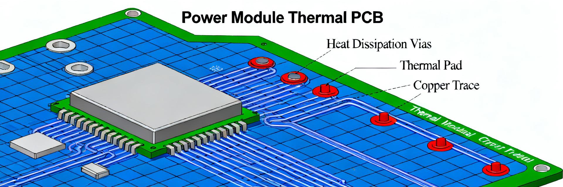
Pinout & Package Details
The LQFP-100 pinout groups channel inputs to facilitate clean high-voltage routing. Key integration steps:
- Creepage & Clearance: Maintain minimum spacing between HV traces based on IPC-2221 standards.
- Grounding: Use a dedicated ground pour with thermal vias under the device to manage heat and signal integrity.
- Buffering: Place high-impedance FET-input buffers as close to the AD45336 sense pins as possible to minimize parasitic capacitance.
Design Checklist & Decision Guide
Before moving to production, verify the following:
- [ ] Absolute max input voltage derated to <180V for safety?
- [ ] Buffer amplifier input bias current <50pA to limit offset?
- [ ] PCB layout includes high-voltage keepout areas around input pins?
- [ ] Thermal simulation confirms junction temperature <85°C at max load?
Summary
- The AD45336 offers 32 channels with 5.2 MΩ resistance and ±10 ppm matching for precision high-voltage scaling.
- High source impedance necessitates careful selection of low-noise, low-bias buffer amplifiers.
- PCB layout must prioritize creepage/clearance and thermal management for the LQFP-100 package.
Frequently Asked Questions
How to interpret AD45336 datasheet voltage and power limits?
Read absolute maximum ratings and per-channel dissipation in the datasheet, then apply a safety margin (commonly 15–25%). Calculate power per channel as P = V^2 / Rseries at the expected max input, confirm package thermal resistance, and validate with thermal simulations to ensure operation within −10 °C to +85 °C.
What are practical steps to test AD45336 resistor divider performance?
Use a precision source and high-resolution DMM to apply known voltages and log outputs. Measure per-channel series resistance with an LCR meter at low excitation. Perform temperature cycling to capture drift and compare results to the official datasheet tables.
What PCB layout tips help when using AD45336 pinout?
Maintain generous creepage/clearance for high-voltage traces, isolate HV channels from digital signals, and use a continuous ground pour. Provide test pads for early debug and keep traces short from device pins to buffers to minimize parasitics.
When should designers choose AD45336 over discrete networks?
Choose the AD45336 when multi-channel (32-ch) density is required alongside tight ratio matching (±10 ppm) that is difficult to achieve with discrete resistors. It reduces BOM complexity and ensures long-term stability for high-voltage sensing up to 225V.