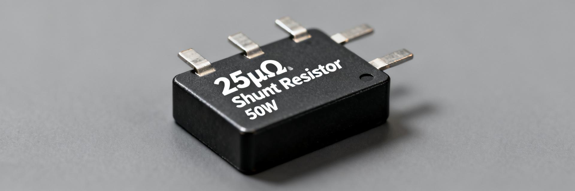
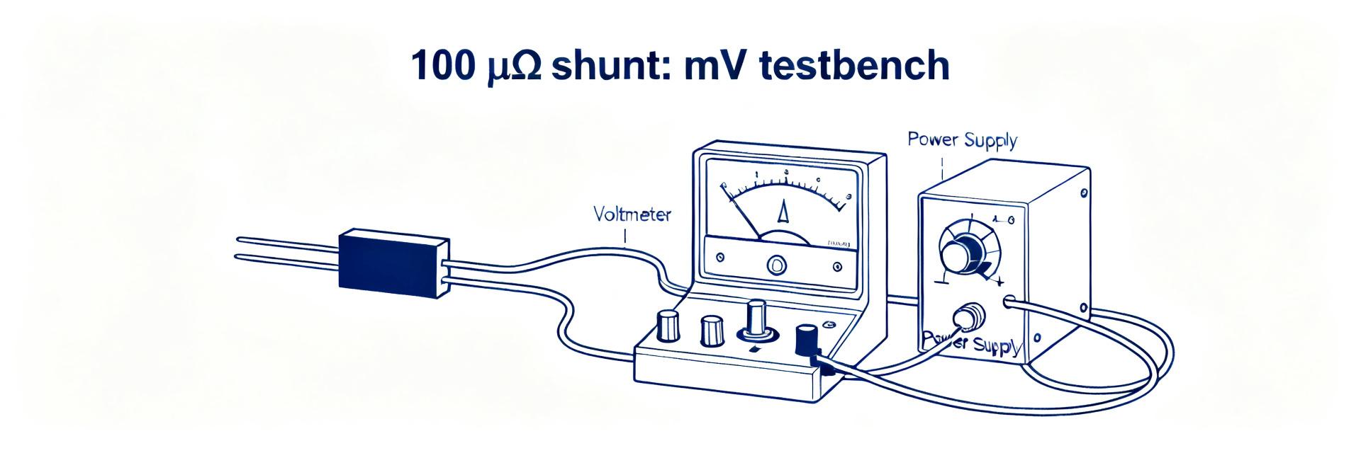
ORNTA1002ZUF datasheet: full specs, footprint & dimensions
The ORNTA1002ZUF is summarized here with the most critical measured specs up front: package length ≈ 4.93 mm (0.194 in), width ≈ 3.99 mm (0.157 in), seated height ≈ 1.73 mm (0.068 in), lead/pin pitch 1.27 mm (0.050 in), power per element ≈ 100 mW, total package ≈ 400 mW. This single-page, engineering-ready breakdown of the ORNTA1002ZUF datasheet lets designers verify specs, generate a PCB footprint, and validate mechanical fit quickly; note the brief mention of specs and footprint here as orientation.
Purpose: condense the datasheet into actionable sections for PCB layout, assembly, and pre-production verification. The following sections present a compact product snapshot, full electrical and performance data, a practical mechanical/footprint table, PCB land-pattern guidance, implementation tips, and a concise pre-production checklist to shorten the turn from design to validated spin.
Quick product snapshot (background)
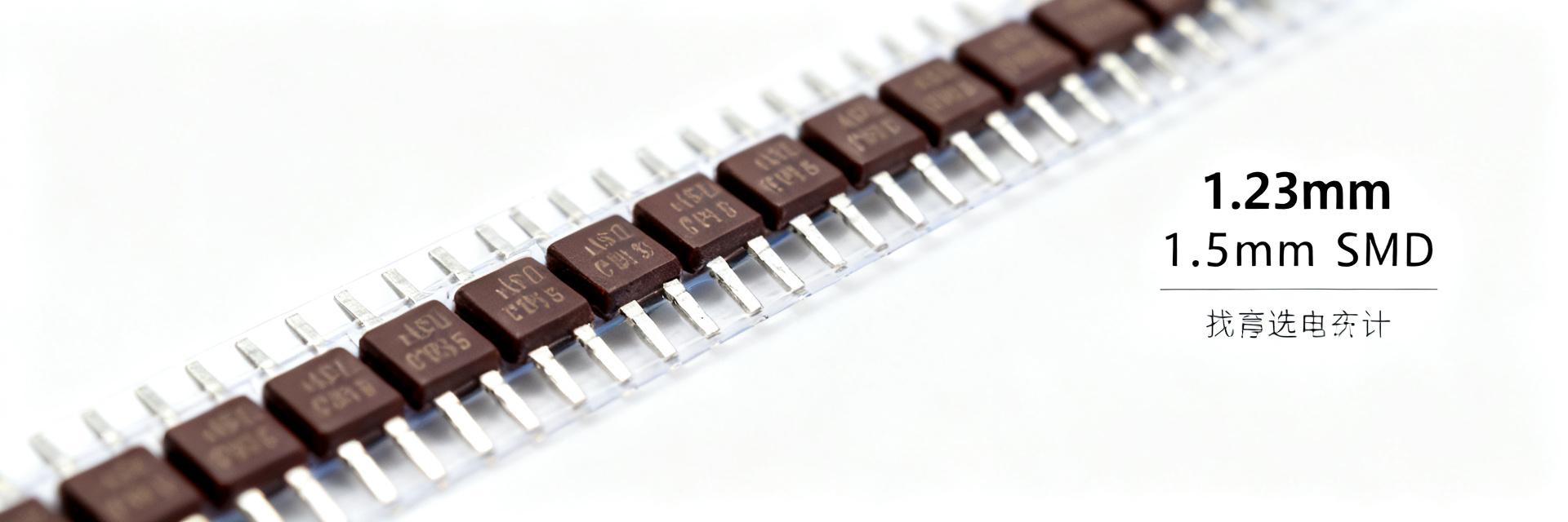
Point: concise identity and context for selection. Evidence: this part is a low-profile, multi-element thin-film resistor array with a small 1.27 mm pitch aimed at space-constrained PCBs. Explanation: it suits compact divider or resistor-array uses where matched elements and thermal behavior matter; observe the limited per-element power rating when planning thermal relief and copper pours.
At-a-glance table
| Parameter | Value |
|---|---|
| Package type | Small molded SMD array |
| Element count | 4 elements (array) |
| Pitch (lead) | 1.27 mm (0.050 in) |
| Power per element | ≈ 100 mW |
| Total package power | ≈ 400 mW |
| Typical tolerances | ppm-level matching; verify datasheet for percent tolerances |
| Max seated height | 1.73 mm (0.068 in) |
When to use this part (short guidance)
- Precision divider/array where matched resistance and low parasitics are needed on tight PCBs.
- Low-power signal conditioning on compact modules; not intended for high dissipation.
- Space-constrained designs requiring a small footprint and predictable thermal behavior.
Full electrical specifications (data deep-dive)
Point: electrical specs drive selection. Evidence: nominal resistance values, tolerances, and TCR dictate accuracy and stability. Explanation: designers should confirm available nominal values and tolerance options in the official datasheet; typical thin-film arrays provide tight tolerances and low TCR, enabling stable divider ratios across temperature but still requiring verification for precision designs.
Resistance values, tolerances & temperature coefficients
Point: matching and TCR affect divider accuracy. Evidence: these arrays commonly offer a range of nominal resistances and tight matching between elements. Explanation: check the datasheet table for exact resistance options and matching/tracking specs; typical TCRs are low (tens of ppm/°C) but thermal tracking is the relevant metric when using the array as a multi-element divider.
Power, limits and derating curves
Point: thermal limits are the controlling design constraint. Evidence: per-element ≈ 100 mW and total ≈ 400 mW define safe operating envelope; derating with ambient temperature and PCB copper area is required. Explanation: apply derating curves from the datasheet, distribute copper pours to spread heat, and avoid concentrating dissipation in single elements beyond their rating.
Performance & reliability data (data analysis)
Point: long-term and test performance determine fit for critical applications. Evidence: noise, stability, and drift are specified under controlled test conditions; lifecycle tests such as thermal shock and solderability are listed. Explanation: review the maximum operating temperature range and long-term drift figures in the datasheet when designing measurement or calibration systems that rely on stable divider ratios.
Electrical performance & test limits
Point: noise and drift influence precision. Evidence: test conditions (temperature/humidity) and limits are specified to define typical behavior. Explanation: use the datasheet’s test condition notes to interpret stability numbers; if the application requires ppm-level stability over years, allocate margin or calibration steps accordingly.
Environmental & lifecycle ratings
Point: assembly and field reliability depend on environmental ratings. Evidence: datasheet sections usually list thermal shock, moisture sensitivity, and solderability details. Explanation: for high-reliability designs, confirm MSL and thermal cycling data and require lot traceability from procurement before volume buys.
Footprint & mechanical dimensions (practical reference)
Point: accurate mechanical data is essential for CAD and assembly. Evidence: critical dims include overall length, width, pitch, seated height, and pad/lead width. Explanation: use the table below to place pads and verify tolerances; this supports creation of an ORNTA1002ZUF footprint and 3D model for fit checks in the enclosure.
Full mechanical dimension table (mm + inches)
| Dimension | mm | inch |
|---|---|---|
| Overall length (A) | 4.93 mm | 0.194 in |
| Overall width (B) | 3.99 mm | 0.157 in |
| Pin/lead spacing (C) | 1.27 mm | 0.050 in |
| Seated height (D) | 1.73 mm | 0.068 in |
| Pad/lead width (recommended) | 0.60 mm | 0.024 in |
Recommended PCB land pattern & 3D model guidance
Point: pad geometry affects solder fillets and pick-and-place. Evidence: for 1.27 mm pitch devices, moderate pad length and soldermask clearance improve yields. Explanation: recommend pad width ≈ 0.6 mm, pad length ≈ 1.0 mm, soldermask openings slightly reduced for paste control, and include a clear orientation marker in silkscreen; export a STEP model and validate with a 3D mockup before finalizing the board.
PCB implementation & assembly tips (method guide)
Point: correct assembly avoids rework. Evidence: reflow compatibility and flux recommendations are specified for SMD resistor arrays. Explanation: follow a standard Pb‑free reflow profile with time above liquidus ~30–60 s and peak ~245–260 °C (473–500 °F) depending on vendor guidance; use compatible flux and avoid excessive localized copper that can overheat elements.
Soldering and reflow profile considerations
Point: thermal exposure must be controlled. Evidence: datasheet reflow notes and maximum temperature ratings define process windows. Explanation: set ramp rates and soak zones per the part’s assembly recommendations and prefer reflow over hand soldering for consistent joint quality; confirm solderability data in the datasheet for your chosen flux and paste.
Layout best practices and troubleshooting
Point: routing and copper shapes impact thermal and mechanical performance. Evidence: recommended layout practices mitigate tombstoning and stress. Explanation: route non-critical traces away from the body, use thermal reliefs or poured copper to distribute dissipation evenly, and verify fillets after assembly. Common issues include insufficient paste, misaligned pads, and too-tight silkscreen over pads.
Example use case & procurement/testing checklist (case + action)
Point: validate the footprint before the production run. Evidence: a short example layout section includes pad dimensions and orientation marker. Explanation: create a PCB section with the recommended pads, place a 3D STEP model, and perform a fit test; inspect solder joints optically and via X-ray where applicable.
Reference footprint implementation (mini case)
Point: verification steps shorten debugging. Evidence: dimension check and fit test confirm mechanical compatibility. Explanation: after placing the 3D model on the board, print a 1:1 paper outline for a mechanical fit check, then assemble a small batch to confirm soldering behavior and electrical continuity before committing to panels.
Pre-production checklist & testing steps
- Validate footprint with 3D mockup and a hand-fit inspection.
- Run a small assembly build: reflow, inspect solder fillets, check resistances and matching at ambient and elevated temperatures.
- Confirm lot traceability, datasheet revision, and any packaging changes before volume procurement.
Summary
- The ORNTA1002ZUF datasheet supplies the critical mechanical and electrical specs required to create a validated PCB land pattern and assembly flow; confirm the package length 4.93 mm, width 3.99 mm, seated height 1.73 mm, and 1.27 mm pitch when modeling the footprint.
- Respect per-element power ≈100 mW and total package ≈400 mW: distribute copper to manage heat and follow derating guidance to avoid long-term drift and degradation.
- Follow recommended pad sizes (≈0.6 mm × 1.0 mm), include a clear orientation marker, export a STEP for fit checks, and complete the pre-production checklist prior to first spin.
FAQ
What dimensions should I verify when checking the footprint?
Verify overall length, width, seated height, lead pitch, and pad width against the mechanical table. Check tolerances called out for critical dimensions and confirm the 3D model fits inside any enclosure features; a physical or printed 1:1 check prevents costly re-spins.
How should I manage thermal dissipation for the resistor array?
Spread heat with copper pours tied to the pads, use thermal reliefs where needed, and follow derating guidance from the datasheet. Avoid concentrating dissipation in a single element and validate with thermal probes or IR imaging during prototype testing.
What inspection and test steps are recommended before volume production?
Perform optical inspection for solder fillets, X-ray for hidden joint defects if available, electrical verification of resistor values and matching, and thermal cycling or burn-in as required by your reliability needs. Confirm supplier datasheet revision and lot traceability before bulk orders.
What are the baseline power limits of the ORNTA1002ZUF?
The power rating is approximately 100 mW per resistor element, with a maximum limit of 400 mW total for the entire package. Designers must apply standard thermal derating based on the ambient operating temperature.