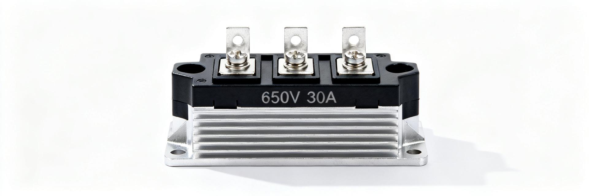
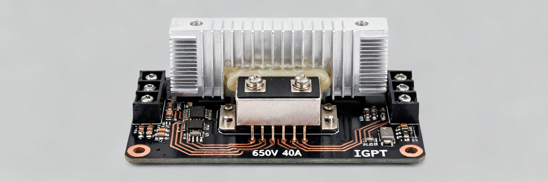
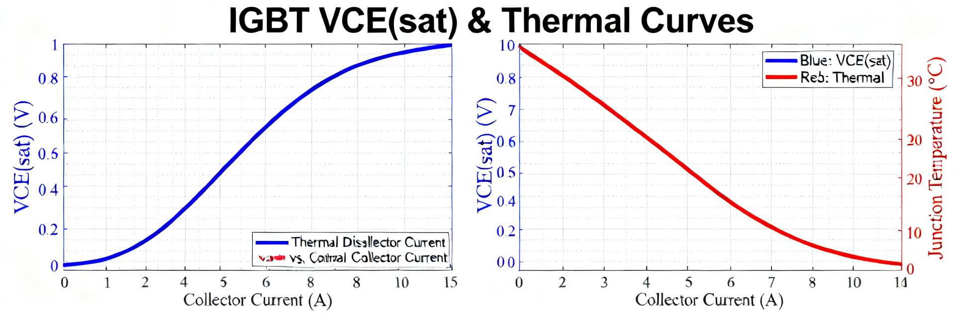
IGBT Specs Explained: Key Datasheet Metrics & Limits
Designers rely on a clear read of an IGBT datasheet to avoid catastrophic failures; modern devices list voltages from a few hundred volts to multi‑kV and pulsed currents of thousands of amps, yet many mistakes come from misreading tables. This introduction uses the term IGBT datasheet to frame what to extract and why those numbers determine protection, thermal design, and reliability.
Point: a concise, data‑driven read reduces prototype iterations. Evidence: typical datasheets separate electrical, thermal, and switching data. Explanation: extracting the right metrics up front shortens design cycles and prevents repeated lab failures by focusing tests on the true limits rather than optimistic typicals.
1 — Background: What an IGBT Datasheet Contains and Why It Matters
Core sections you’ll always see
Point: datasheets group information into predictable sections. Evidence: common headings include electrical ratings, thermal data, switching characteristics, SOA/graphs, and packaging/pinout. Explanation: each section maps directly to design actions—electrical ratings set component selection, thermal data drives heatsink choice, switching specs inform gate driver design and EMI mitigation.
“Limits” vs. recommended operating conditions: why the distinction matters
Point: absolute maximum ratings and recommended operating conditions are distinct. Evidence: absolute maximums are single‑point failure boundaries; recommended conditions define safe continuous operation. Explanation: exceeding an absolute maximum can cause immediate failure, while running at recommended conditions preserves lifetime—designs must derate for real ambient and transient conditions.
2 — Data Deep-Dive: Absolute Maximum Ratings — Definitions & Typical Ranges
Absolute maximum ratings: definitions and measurement conditions
Point: absolute maximum ratings are the non‑negotiable device boundaries. Evidence: these include VCES, VGE limits, Ic (continuous), Icp (pulse), Tj_max, and Pd, often given for Tc=25°C or Ta=25°C test conditions. Explanation: Tc‑based numbers assume perfect heat sinking; Ta‑based numbers reflect free‑air conditions—using the wrong baseline will underestimate stress by tens of percent.
Typical numeric ranges and what they imply for design
Point: voltage class dictates related protections. Evidence: low‑voltage IGBTs (~600–1200 V) commonly target inverters; mid (1.2–3.3 kV) and high (>3.3 kV) modules have higher SOA constraints. Explanation: higher voltage devices need snubbers, avalanche energy handling, larger creepage clearance, and more conservative current derating to avoid secondary breakdown and excessive junction heating.
3 — Key IGBT Datasheet Metrics You Must Extract (IGBT datasheet)
| Parameter | Symbol | Domain | Critical Impact on Design |
|---|---|---|---|
| Collector-Emitter Voltage | VCES | Static | Sets dynamic blocking voltage margin & protection limits |
| Continuous Collector Current | IC | Static | Determines continuous load handling and thermal losses |
| Gate-Emitter Threshold | VGE(th) | Static | Governs turn-on bias point and noise margins |
| Gate Charge | Qg | Dynamic | Sizes peak current requirements for gate drive circuit |
| Thermal Resistance (Junction-to-Case) | RthJC | Thermal | Dictates heatsink size & thermal dissipation efficiency |
Static metrics to capture (Vces, Ic, Vge(th), RthJC)
Point: static metrics form the steady‑state basis for design. Evidence: capture VCES(max), continuous Ic, VGE threshold, saturation VCE(sat), and thermal resistances RthJC/RthJA. Explanation: use VCE(sat) and Ic for conduction losses, and RthJC with Pd to compute junction rise: Tj = Tc + Pd × RthJC (single‑device) or Tj = Ta + Pd × RthJA for board‑level estimates.
Dynamic and switching specs (turn-on/off times, Qg, dv/dt, di/dt)
Point: switching metrics determine driver and EMI choices. Evidence: parameters include ton/toff, Qg, Cies/Cres/Coss, dv/dt and di/dt limits, often with test circuits noted. Explanation: compute switching energy Esw from known V, I, and measured transition times, and select gate driver current and resistor to trade switching loss versus EMI—use Qg and driver voltage to size drive current.
4 — Reading Absolute Maximum Ratings & Limits on the Datasheet (IGBT datasheet)
Common pitfalls: ambient vs. case temperature, single-pulse vs. repetitive
Point: temperature baselines and pulse definitions are frequent traps. Evidence: some ratings use Tc=25°C single‑pulse avalanches; others specify repetitive pulse energy at elevated Tj. Explanation: convert Tc ratings to Ta contexts by accounting for thermal path; treat single‑pulse acceptance as short‑term only and avoid extrapolating to continuous duty without thermal re‑evaluation.
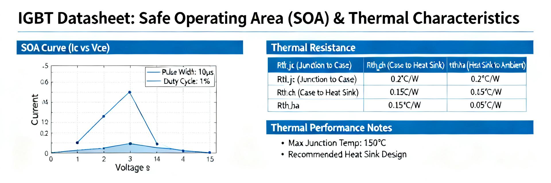
Interpreting derating curves and SOA (Safe Operating Area)
Point: derating curves translate graphs into allowable operating points. Evidence: SOA plots show current limits versus voltage at given pulse durations and temperatures. Explanation: determine permissible current by reading SOA at your target VCE and pulse width, then apply thermal resistance and ambient rise to ensure junction stays below Tj_max with margin.
5 — Practical Design & Verification Checklist (methods to stay inside limits)
Thermal management: junction temp calculations, heatsink selection, and transient thermal limits
Point: thermal design prevents runaway. Evidence: required values include RthJC, RthJA, allowable Pd and Tj_max. Explanation: calculate steady‑state Tj = Ta + Pd × RthJA, select a heatsink such that RthJA_total = (Tj_target − Ta)/Pd, and add a 10–20% safety margin to accommodate measurement and production variability.
Switching protection: gate resistor sizing, snubbers, TVS/RC, and soft-start
Point: protect against overvoltage and dv/dt stress. Evidence: use Qg, Cgd/Cgs, dv/dt and VGE(max) from the datasheet. Explanation: choose gate resistor to limit dV/dt and peak di/dt per driver capability, design RC snubber or active clamp to absorb energy, add TVS for transients, and implement soft‑start to limit inrush energy during commissioning.
6 — Failure Modes, Debugging, and Prototype Tests (case + action)
Top failure modes when limits are exceeded
Point: specific misapplied specs map to predictable failures. Evidence: overvoltage leads to avalanche damage, thermal overstress causes bond lift or solder fatigue, gate overdrive causes latch or oxide breakdown. Explanation: track each failure back to the specific datasheet metric—e.g., repeated avalanche beyond single‑pulse energy indicates SOA misinterpretation or inadequate snubber energy capacity.
Quick lab checklist: how to validate datasheet limits on a prototype
Point: staged validation reduces risk. Evidence: perform current‑limited bench tests, single‑pulse stress, repetitive stress with thermal monitoring, and IR or thermocouple junction measurements. Explanation: start with low duty and single pulses, measure VCE and Tj, compare to calculated values, then increase load within margins; record pass/fail criteria and instrument points for reproducibility.
Summary
Point: concise, actionable recaps help prevent repeat errors. Evidence: three core actions cover most failures. Explanation: extract static, dynamic, and thermal metrics from the IGBT datasheet; treat absolute maximum ratings as hard limits and derate for real thermal conditions; and validate designs with governed prototype tests and conservative margins to catch SOA and transient issues before production.
Key Summary
- Extract static (VCE(sat), Ic, RthJC), dynamic (Qg, ton/toff), and thermal metrics from the IGBT datasheet to size conduction, drive, and cooling systems accurately.
- Treat absolute maximum ratings and SOA graphs as non‑negotiable; convert Tc‑based tests to real‑world Ta conditions and apply at least 10–20% derating for reliability.
- Validate with staged prototype tests: single‑pulse, current‑limited repetitive testing, and junction temperature monitoring to confirm theoretical calculations and safety margins.
Frequently Asked Questions
How should an engineer read an IGBT datasheet for thermal design?
Start by capturing RthJC and RthJA, Pd limits, and Tj_max. Calculate steady‑state junction temperature using Tj = Ta + Pd × RthJA or Tj = Tc + Pd × RthJC if using case temperature. Select a heatsink such that calculated Tj remains below Tj_max with a safety margin of 10–20%.
How can switching loss be estimated from datasheet numbers?
Estimate switching loss by integrating voltage and current over transition times: Esw ≈ 0.5 × V × I × (ton + toff) for trapezoidal approximations, scaled by switching frequency. Use Qg and driver capability to size gate drive current, which affects transition times and therefore Esw.
What test steps validate absolute maximum ratings without risking equipment?
Use current‑limited supplies, start with single‑pulse tests at low duty, monitor junction temperature with IR or thermocouples, and progress to repetitive pulses only after confirming thermal stability. Define pass/fail thresholds beforehand, and include emergency shutoff parameters to protect the DUT and bench.
What is the primary difference between case (Tc) and ambient (Ta) temperature ratings?
Case-based (Tc) ratings assume a perfect thermal contact with an infinite heatsink, ideal for heavy cooling module designs. Ambient-based (Ta) ratings assume free-air natural convection, which results in a much higher thermal resistance and requires severe current and power derating.