IGBT Module Datasheet Deep-Dive: MITF35R12P2STL-BP Specs
The MITF35R12P2STL-BP is rated in the 1200 V class with a continuous collector current headline of about 35 A at Tc = 100°C, making it a candidate for medium-power inverters and motor drives. This article teaches engineers how to read the module datasheet, extract the numbers that drive thermal and switching design, validate performance on the bench, and apply those numbers in real designs for robust system-level choices.
Point: Quick orientation helps prioritize what to copy from the official datasheet into a design spreadsheet. Evidence: the two headline numbers above (1200 V VCES, ~35 A @ Tc=100°C) appear in the manufacturer’s ratings table. Explanation: use those as gating constraints for bus voltage, continuous current margin, and thermal design before deeper switching and SOA checks.
1 — Module at a glance: identity, topology and headline specs (background)
1.1 Part breakdown & naming convention
Point: Part names encode class information that speeds selection. Evidence: MITF35R12P2STL-BP breaks into current class (35), voltage class (12 = 1200 V), and package/topology suffixes. Explanation: read the code to confirm you picked a half-bridge/six-pack option and the package style; this determines terminal layout, mounting bolt pattern, and whether the module includes integrated diodes or gate-emitter features required by your driver.
1.2 Headline electrical specs summary
Point: Pull the critical electrical limits immediately into a one-line table for review. Evidence: datasheet lists VCES, Ic (Tc reference), ICM/pulsed ratings, Pd, and allowed temperature ranges. Explanation: these drive bus selection, derating, and heatsink needs; keep the quick reference table beside simulation and layout work.
| Spec | Value (typical / note) |
|---|---|
| VCES | 1200 V |
| Ic (cont.) | ≈35 A @ Tc = 100°C |
| Pd (per module) | See datasheet Tc-referenced curves |
| Thermal interface | Cu baseplate, torque & insulator per datasheet |
2 — Absolute maximum ratings & thermal limits (datasheet deep-dive) (data analysis)
2.1 Voltage, current and power dissipation limits
Point: Understand absolute vs. operational limits to avoid overstress. Evidence: the datasheet shows VCES and VCE(sus) absolute max, continuous Ic at a Tc reference, and pulsed/peak Ic or ICM values. Explanation: use absolute ratings only for fault analysis; design operating points using derated currents and power dissipation at your expected case temperature, not absolute maxima.
2.2 Thermal resistances, junction temps & mounting considerations
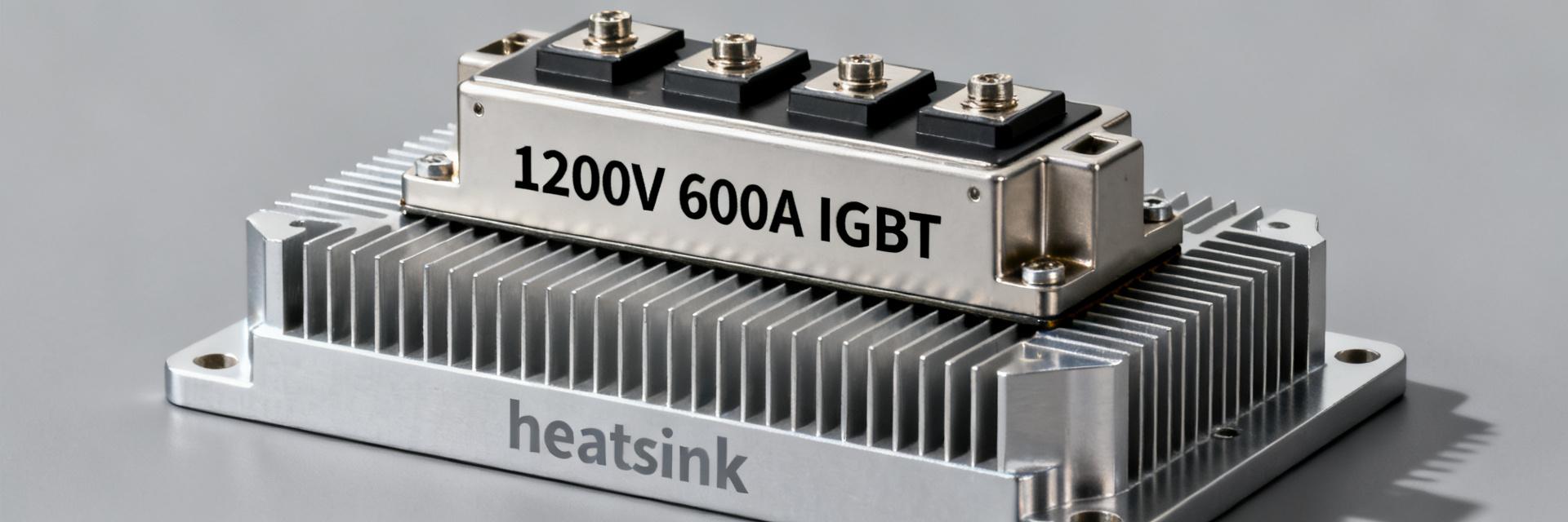
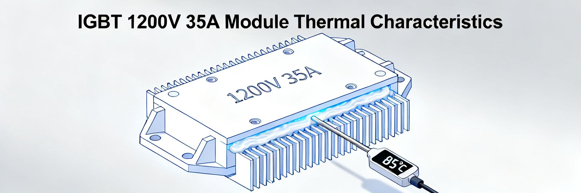
Point: Thermal resistances and mounting notes determine heatsink selection and assembly practice. Evidence: the datasheet provides Rth(j‑c) and Rth(c‑s) and specifies Tc measurement points and mounting torque; consult the MITF35R12P2STL-BP datasheet for exact numbers. Explanation: combine Rth(j‑c)+Rth(c‑s)+Rth(hs‑a) to budget junction rise; follow torque and insulator instructions to avoid degraded thermal contact or baseplate warping.
3 — Switching characteristics & dynamic behavior (data analysis)
3.1 Gate characteristics, switching energy and losses
Point: Switching and gate specs let you estimate dynamic losses. Evidence: datasheet lists gate threshold, recommended VGE, and typically Eon/Eoff curves at representative VCE and IC points. Explanation: worked example — for a phase current of 16 A and Vdc 400 V, assume VCE(on) ≈1.2 V (typical device figure) giving Pcond ≈1.2·16 = 19.2 W per IGBT; if Eon+Eoff ~0.5 mJ at these conditions and fsw = 8 kHz, Psw ≈0.0005·8000 = 4 W; total ≈23.2 W per device. Use the datasheet’s actual Eon/Eoff points to replace assumptions in your spreadsheet.
3.2 Safe operating area (SOA), short‑circuit capability and reliability constraints
Point: SOA and short‑circuit time define protection strategy. Evidence: the datasheet includes SOA graphs and short‑circuit time or energy limits under specified gate and cooling conditions. Explanation: interpret the SOA envelopes at your VCE and pulse widths; design driver dead‑time, current sensing, and fast protection so single‑device stresses never cross the SOA or exceed short‑circuit time without intervention.
4 — How to validate datasheet claims: measurement & test best practices (method/guide)
4.1 Test setups: thermal, static and switching measurements
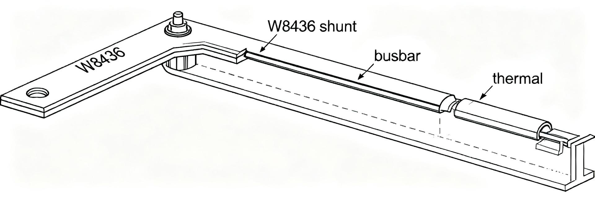
Point: Reproduce datasheet conditions before trusting numbers. Evidence: the official datasheet specifies Tc reference, gate waveform, and test circuits for static and dynamic parameters. Explanation: use Kelvin current shunts for Ic/Vce, place a thermocouple at the Tc point shown in the datasheet, and match gate drive amplitude and rise/fall conditions to reproduce Eon/Eoff curves; document test conditions in your records for traceability.
4.2 Interpreting waveforms and thermal imaging
Point: Match waveform shapes to expected losses and spot mechanical/thermal issues. Evidence: switching waveforms and thermal images are used in independent lab verification to confirm vendor claims. Explanation: look for excessive overshoot or abnormal dV/dt; use thermal imaging to confirm hotspots and verify calculated Rth values — watch for degraded TIM or mounting issues if local temperatures exceed predictions.
5 — Integration example: motor-drive/inverter design using MITF35R12P2STL-BP (case study)
5.1 Sizing gate driver, heatsink and DC bus
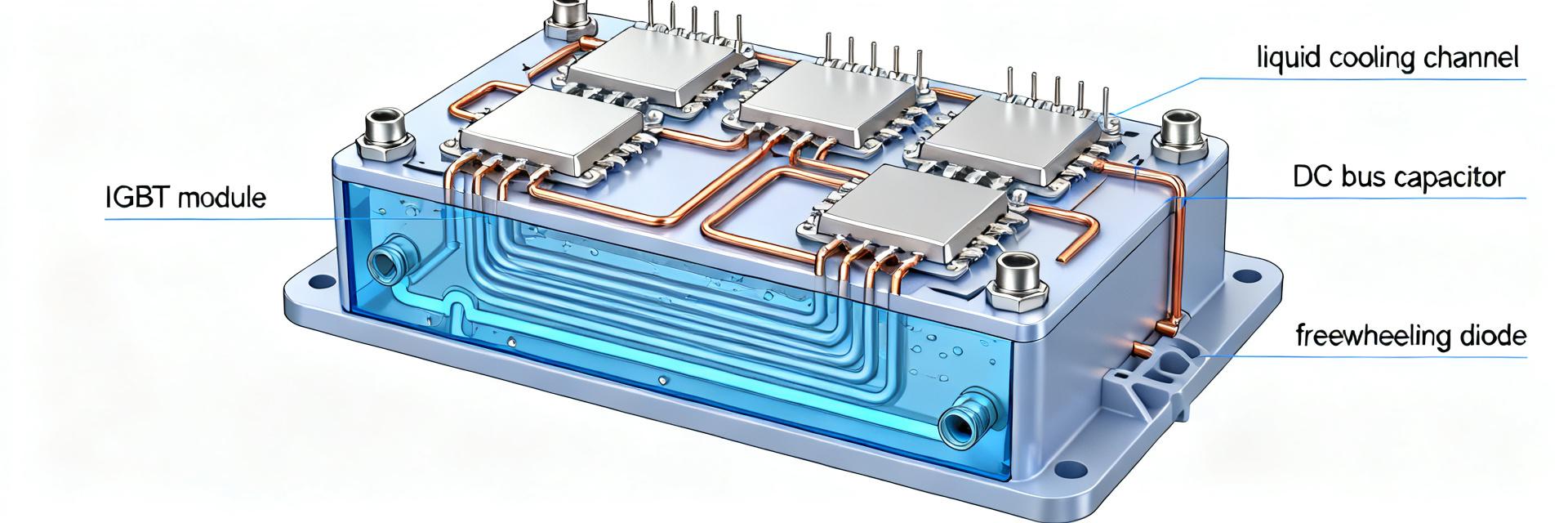
Point: Translate losses into a heatsink spec. Evidence: from the worked-loss example above (~23.2 W per IGBT at 16 A, 400 V, fsw=8 kHz). Explanation: required thermal headroom ΔT = Tc_target − Tamb. For Tc_target = 75°C and Tamb = 40°C, ΔT = 35°C; Rth_total_allowed = 35°C / 23.2 W ≈ 1.5°C/W. Subtract Rth(c‑s) and Rth(j‑c) from datasheet to pick Rth(hs‑a). Size driver capability for gate charge and peak gate current per the datasheet gate charge table and include snubber/clamp components sized from transient energy limits.
5.2 Layout, EMC and paralleling considerations
Point: Mechanical and EMC choices affect losses and reliability. Evidence: datasheet package and terminal drawings show busbar attachment points and recommended series inductance mitigation. Explanation: use short, wide busbars, tightly looped gate‑emitter wiring, and symmetrical parasitics if paralleling. When paralleling, anticipate current imbalance and include small series resistances or matched gate resistors to improve sharing.
6 — Design checklist & action items for engineers (action)
6.1 Pre‑design checklist
- Confirm VCES margin vs. system bus (1200 V class) and select derating target.
- Verify continuous Ic margin at your expected Tc and apply thermal derating.
- Record Rth(j‑c) and Rth(c‑s) from the official datasheet into design spreadsheet.
- Specify gate drive voltage, peak current, and gate resistor strategy from gate charge data.
- Plan fast protection for OC/SC and confirm SOA margins in worst‑case transients.
6.2 Procurement & qualification checklist
- Confirm supplier traceability and exact datasheet revision for procurement records.
- Capture lot/serial traceability and handling instructions (ESD, bolt torque, TIM).
- Specify environmental and thermal cycling tests for qualification builds.
Summary
- The MITF35R12P2STL-BP is a 1200 V, ≈35 A class IGBT module; use these headlines to screen system suitability and initial thermal budgets.
- Extract Rth and Eon/Eoff from the official datasheet, then reproduce test conditions on the bench to validate switching and thermal behavior.
- Perform loss budgeting (conduction + switching) to derive an allowable Rth(hs‑a); follow mounting and torque notes to preserve thermal contact.
Frequently Asked Questions
How does an IGBT module datasheet guide bench validation?
Point: The datasheet defines test conditions you must replicate. Evidence: Tc reference, gate drive waveforms, and measurement points are specified. Explanation: match those conditions on the bench to confirm VCE(on), Eon/Eoff, and thermal resistance; discrepancies indicate assembly, TIM, or measurement errors that must be resolved before qualification.
Can the MITF35R12P2STL-BP be paralleled for higher current?
Point: Paralleling is possible but requires caution. Evidence: module thermal and dynamic specs plus package parasitics affect sharing. Explanation: ensure matched gate drive timing and consider small series resistances, balanced busbar inductance, and thorough testing for current sharing under steady and transient conditions before production use.
What are the first bench tests to confirm datasheet numbers?
Point: Start with static and thermal verification. Evidence: datasheet supply of Ic/Vce and Rth references. Explanation: measure VCE at rated Ic with Kelvin sense and Tc thermocouple, reproduce switching test points (Vdc, Ic, gate drive) to measure Eon/Eoff, and use thermal imaging to confirm calculated junction and case temperatures in your mounting configuration.
Why is thermal interface material (TIM) critical for this module?
Point: Proper TIM application ensures minimal contact resistance. Evidence: Rth(c-s) is highly dependent on mounting quality. Explanation: Incorrect torque or poor TIM coverage creates air gaps, leading to localized hotspots, increased junction temperature, and potential premature failure despite correct electrical operation.