Datasheet Deep Dive: Infineon F3L340R12W3H7H11BPSA1 IGBT Performance Analysis
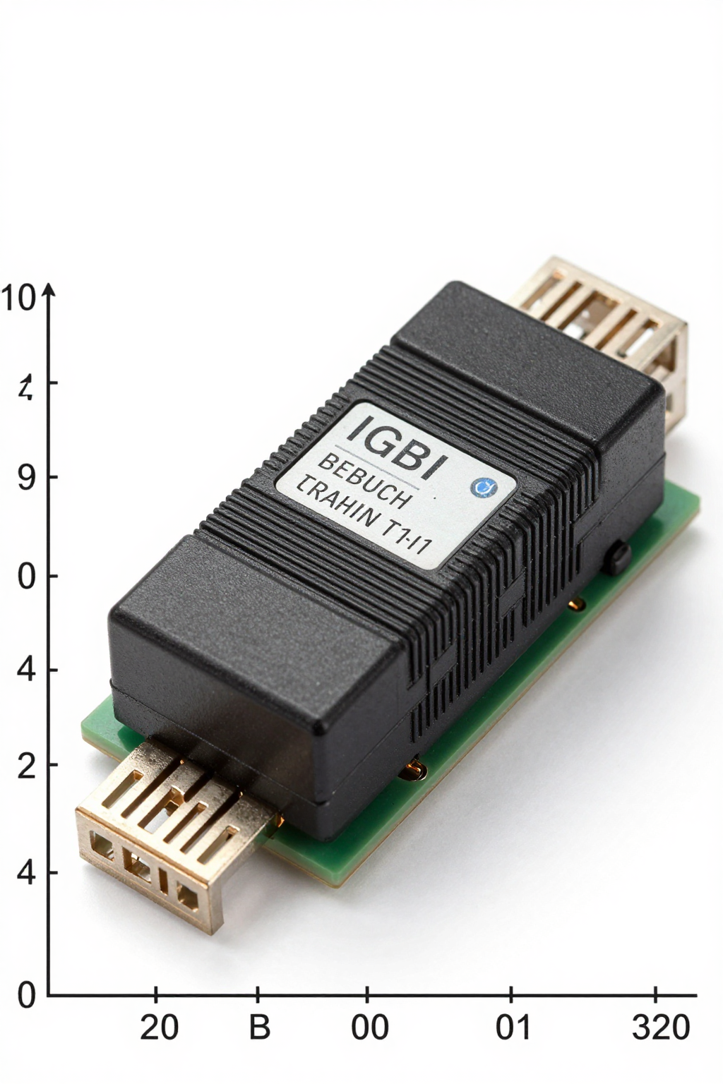
In high-power industrial applications, efficiency isn't just a metric—it's the bottom line. The Infineon F3L340R12W3H7H11BPSA1 IGBT module promises a 1200V/340A performance envelope with ultra-fast switching characteristics. But does the data support its claim as a superior choice for three-level inverter topologies? This analysis breaks down the key electrical parameters to determine if this component meets your design requirements.
Core Electrical Specifications & Topology Fit

Voltage and Current Ratings Breakdown
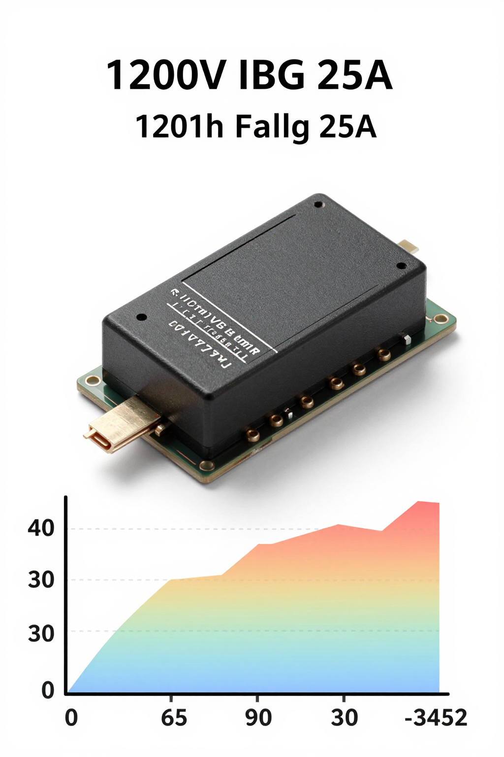
You are looking at a robust power device designed for demanding environments. The module features a collector-emitter voltage rating ($V_{CES}$) of 1200V, providing ample headroom for DC bus voltages up to 800-900V typical in industrial drives. The nominal current rating is 340A at a case temperature of 25°C, dropping to approximately 235A at 80°C. You must consider these thermal derating curves carefully when sizing your cooling system.
| Parameter | Value | Condition |
|---|---|---|
| $V_{CES}$ | 1200 V | Max |
| $I_C$ (Nominal) | 340 A | @ $T_C = 25^\circ\text{C}$ |
| $I_C$ (Derated) | 235 A | @ $T_C = 80^\circ\text{C}$ |
Three-Level Inverter Architecture Compatibility
This specific part number indicates a half-bridge configuration optimized for three-level NPC (Neutral Point Clamped) or similar topologies. You will find that the internal layout minimizes parasitic inductance between the main switches and clamping diodes. This architecture reduces harmonic distortion and electromagnetic interference (EMI), which is critical for sensitive motor loads. If you are designing a medium-voltage drive, this topology fit significantly simplifies your filter stage requirements.
Switching Characteristics & Efficiency Metrics
Ultra-Fast Chip Technology Impact on Losses
The core advantage lies in the TRENCHSTOP™ IGBT5 technology. You benefit from reduced tail currents during turn-off, which directly lowers switching losses ($E_{off}$). At a standard test condition of 600V and 340A, the total switching loss is remarkably low compared to previous generations. This efficiency gain translates to less heat generation per cycle, allowing you to push higher frequencies without exceeding thermal limits.
"Lower switching losses enable higher PWM frequencies, improving dynamic response in servo drives." — Industry Best Practice
Thermal Management at High Duty Cycles
Handling high duty cycles requires precise thermal management. The module’s junction-to-case thermal resistance ($R_{thJC}$) is optimized to facilitate efficient heat transfer to your heatsink. You should monitor the maximum junction temperature ($T_{vj,max}$) of 175°C. Exceeding this limit risks irreversible damage. For continuous operation at near-maximum current, ensure your cooling solution can dissipate the calculated power losses, typically around 1.5-2.0 kW depending on frequency.
Practical Design Integration Guidelines
Gate Driver Selection for Optimal Turn-On/Off
Selecting the right gate driver is crucial for unlocking the F3L340R12W3H7H11BPSA1's potential. You need drivers capable of delivering sufficient peak current to minimize Miller effect-induced false triggering. Look for isolated gate drivers with active clamping capabilities. Proper gate resistor selection balances switching speed against EMI; too fast increases noise, too slow increases losses. Aim for a rise/fall time that aligns with your control loop bandwidth.
PCB Layout Strategies for Low Inductance
Parasitic inductance in your PCB layout can cause dangerous voltage spikes during turn-off. You must implement short, wide traces for the power loops. Use multi-layer boards with ground planes close to signal layers to reduce impedance. Place decoupling capacitors extremely close to the gate terminals. A well-designed layout ensures that the actual switching behavior matches the datasheet simulations, protecting both the module and your control circuitry.
Key Takeaways
- The F3L340R12W3H7H11BPSA1 offers a 1200V/340A rating ideal for high-power three-level inverters.
- TRENCHSTOP™ IGBT5 technology significantly reduces switching losses, enabling higher efficiency and frequency operation.
- Proper gate driver selection and low-inductance PCB layout are critical to maximize performance and reliability.
- Thermal management must account for derating at higher case temperatures to prevent junction overheating.
Frequently Asked Questions
What is the primary application for the F3L340R12W3H7H11BPSA1?
This module is primarily designed for industrial motor drives, uninterruptible power supplies (UPS), and renewable energy inverters. Its three-level topology compatibility makes it suitable for applications requiring lower harmonic distortion and higher efficiency than traditional two-level converters.
How do I calculate the expected power losses?
You should use the provided thermal resistance values and switching energy data ($E_{on}$, $E_{off}$, $E_{rec}$) from the datasheet. Multiply these by your operating frequency and current waveforms. Online simulation tools can help model these losses accurately under specific load conditions.
Is an external snubber circuit required?
While the module has low internal inductance, proper PCB layout often eliminates the need for large external snubbers. However, small ceramic capacitors across the gate-emitter terminals are recommended to suppress high-frequency noise and protect the gate oxide layer.
What is the maximum junction temperature rating?
The maximum junction temperature ($T_{vj,max}$) is 175°C. Exceeding this limit risks irreversible damage. Thermal management systems must be sized to dissipate calculated power losses (typically 1.5-2.0 kW depending on frequency) to keep the junction within safe operating areas.