MDP1603220RGD04 Datasheet: 220Ω Resistor Network Specs
The MDP1603220RGD04 appears in this datasheet summary as an isolated eight-element resistor network with a nominal 220Ω value, ±2% tolerance, ~250 mW power per element, ~100 V voltage rating, and a low TCR near ±100 ppm/°C. These numbers make the part a practical choice for compact DIP-mounted pull-ups, LED arrays, and matched divider banks where space and element matching matter.
This introduction highlights the critical electrical and mechanical constraints designers must verify on the datasheet before committing to PCB layout or production. Key checks are absolute tolerance, per-element power limits, maximum working voltage between isolated elements, and the package footprint for 16‑pin DIP mounting.
1 — Product background & quick spec summary (background introduction)
Key specs at a glance
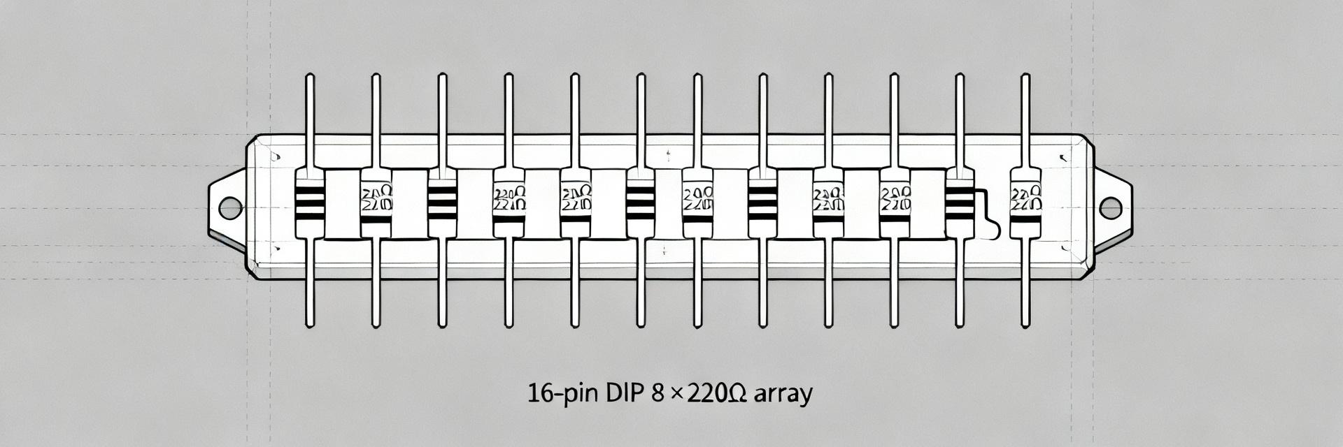
Critical datasheet values: nominal resistance 220Ω; tolerance ±2%; power per element 250 mW; number of resistors 8; configuration isolated; voltage rating ≈100 V; TCR ≈±100 ppm/°C; package 16‑DIP (0.300" / 7.62 mm pitch); typical seated height and lead finish noted in mechanical tables. The MDP1603220RGD04 delivers matched channels with medium precision suited to many multi-channel designs.
| Label | Value | Datasheet location |
|---|---|---|
| Nominal resistance | 220Ω | Electrical specs |
| Tolerance | ±2% | Electrical specs |
| Power per element | 250 mW | Absolute ratings |
| Voltage rating | ≈100 V | Absolute ratings |
| Package | 16‑pin DIP, 0.300" pitch | Mechanical data |
Package, pinout and mechanical notes
The 16‑pin DIP footprint is standard: eight independent resistor bodies with pins paired to each element. PCB footprint should use 0.300" spacing, with recommended pad and keepout dimensions from the mechanical diagrams. Through‑hole mounting provides robust mechanical retention but requires attention to lead bend tolerances and flux cleaning after soldering to avoid long‑term drift.
2 — Electrical performance & limits (data analysis)
Resistance behaviour, TCR and tolerance implications
±2% tolerance sets absolute accuracy bounds; TCR ≈±100 ppm/°C defines temperature sensitivity. Use ΔR = R0 × TCR × ΔT to estimate shift. For a 220Ω element from +25°C to +85°C (ΔT = 60°C): ΔR = 220 × 100e‑6 × 60 = 1.32Ω, so R ≈ 221.32Ω. For matched-channel applications the network often outperforms discrete parts on tracking, even if absolute tolerance is only medium.
Power rating, derating curve and voltage limits
Rated 250 mW per element means I_max = sqrt(P/R) = sqrt(0.25/220) ≈ 33.7 mA, and V_max_element ≈ 7.4 V at that current. Designers should read the datasheet derating curve: typical networks derate linearly above a given ambient temperature to zero at maximum package temperature. The ≈100 V package rating governs isolation between elements and limits series/parallel arrangements for high-voltage designs.
3 — Design & application guidance (method/guideline)
Typical circuit uses & wiring examples
Common uses include pull‑ups/pull‑downs on multi‑input buses, LED array current‑limiting segments, and matched divider banks. Example text schematics: single element used as a pull‑up to 3.3 V; eight isolated elements each tied to separate I/O; series two 220Ω elements for 440Ω limiting (note power splits evenly if matched). Choose isolated networks when independent channels need distinct voltages or when isolation voltage is required.
PCB layout, thermal and reliability tips
Route heavier copper for traces carrying power to a single element to reduce local heating; maintain spacing between channels to limit cross‑heating. Include thermal reliefs for through‑hole pads if wave soldering. In prototypes, measure element temperature under power to confirm derating and perform thermal cycling to reveal solder‑stress induced drift.
4 — Selection, comparison & procurement checklist (case & selection)
Trade-offs: accuracy, power density, and form factor
Checklist: tolerance vs cost (±2% moderate cost), TCR vs stability needs (±100 ppm/°C suitable for non‑precision analog but matched channels are valuable), and power per element vs package size (DIP offers ease of assembly but lower power density than SMD). Compare isolated DIP networks when channel independence and PCB through‑hole robustness outweigh board space savings of SMD arrays.
BOM and procurement checklist
Before ordering confirm package variant and pitch, lead finish, part marking, datasheet revision, RoHS/lead‑free status, and packaging (tube vs tray). Request sample units for first‑run tests, verify shelf life and lifecycle notes, and document alternate suppliers with similar spec sets to mitigate availability risk.
5 — Test procedures and validation (actionable testing + sourcing)
Bench tests to validate datasheet claims
DC resistance: use a 4‑wire method and record multiple elements. TCR: measure at two controlled temperatures and compute ppm/°C from ΔR and ΔT. Power soak: apply rated power to a single element with a current‑limited supply while logging temperature rise with a thermocouple or IR camera. Expected results should align within tolerance and thermal behavior described by the datasheet.
Reliability, compliance and lifecycle considerations
Verify long‑term stability via humidity and thermal cycling tests; check for drift after soldering and conformal coating if the environment requires it. For sourcing, validate the latest datasheet revision, confirm RoHS/REACH declarations, and secure small test quantities before committing to high‑volume buys to reduce lifecycle risk.
Summary
- The MDP1603220RGD04 is an isolated 8‑element 220Ω resistor network with ±2% accuracy and ~250 mW per element, offering matched channels in a 16‑pin DIP ideal for multi‑channel pull‑ups and divider banks.
- Designers must verify TCR (~±100 ppm/°C) effects using ΔR = R0 × TCR × ΔT, confirm power derating for ambient conditions, and respect the ≈100 V isolation rating when arranging series/parallel.
- Before procurement, run basic bench tests (4‑wire resistance, TCR checks, power soak) on samples and confirm package, finish, and datasheet revision to avoid surprises in production.
Common questions
What is the typical current limit for the 220Ω resistor network element?
At 250 mW per element, the continuous current limit is about 33.7 mA (I = sqrt(P/R)). Designers should derate this value with ambient temperature per the datasheet derating curve and avoid sustained operation at or near this limit without thermal validation.
How does the 220Ω resistor network TCR affect precision applications?
With TCR ≈±100 ppm/°C, a 60°C rise results in ≈0.6% change for a 220Ω element (~1.32Ω). For matched‑channel biasing the relative tracking is often better than absolute accuracy, but for tight absolute tolerances designers should consider lower‑TCR networks or matched thin‑film options.
When should an isolated network be chosen over a bussed (common) resistor array?
Choose isolated networks when each resistor must carry different voltages, be used independently, or when isolation voltage between channels is required. Bussed arrays simplify wiring and save PCB pins when a common node is acceptable, but they prevent independent isolation and can complicate matched‑channel layouts.
What critical PCB layout practices prevent long-term drift in the MDP1603220RGD04?
Route heavier copper traces to reduce local heating, maintain physical spacing between channels to prevent cross-heating, apply thermal reliefs for through-hole pads, and perform proper flux cleaning after soldering to avoid contamination-induced drift.