MSP10A014K70GDA Resistor Array: Detailed Spec Report
The MSP10A014K70GDA resistor array appears in many space-constrained analog and pull-network designs due to its 9-element bussed topology and compact 10-pin SIP package. This report-style overview extracts the critical datasheet figures—4.7 kΩ nominal, ±2% tolerance, ~100 ppm/°C TCR, and 200 mW per element—to guide footprint, thermal derating and test planning for practical integration.
According to the part's datasheet, the MSP10A014K70GDA resistor array lists a nominal element value of 4.7 kΩ, ±2% tolerance, 200 mW power per element, a 9-resistor bussed topology, and a TCR on the order of 100 ppm/°C—details that immediately determine thermal derating, PCB footprint, and test requirements.
Background & Part Overview
Part ID, Package and Internal Configuration
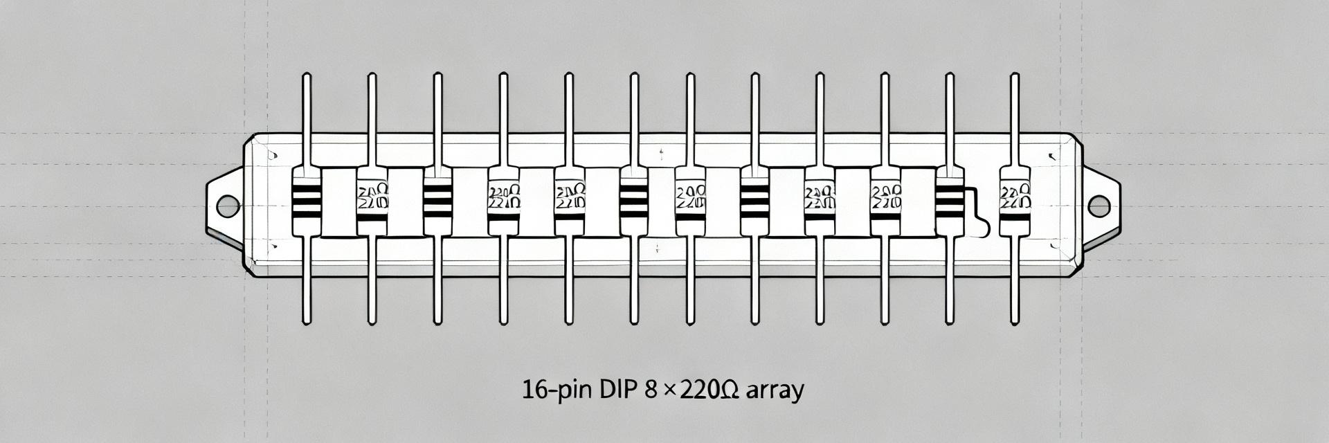
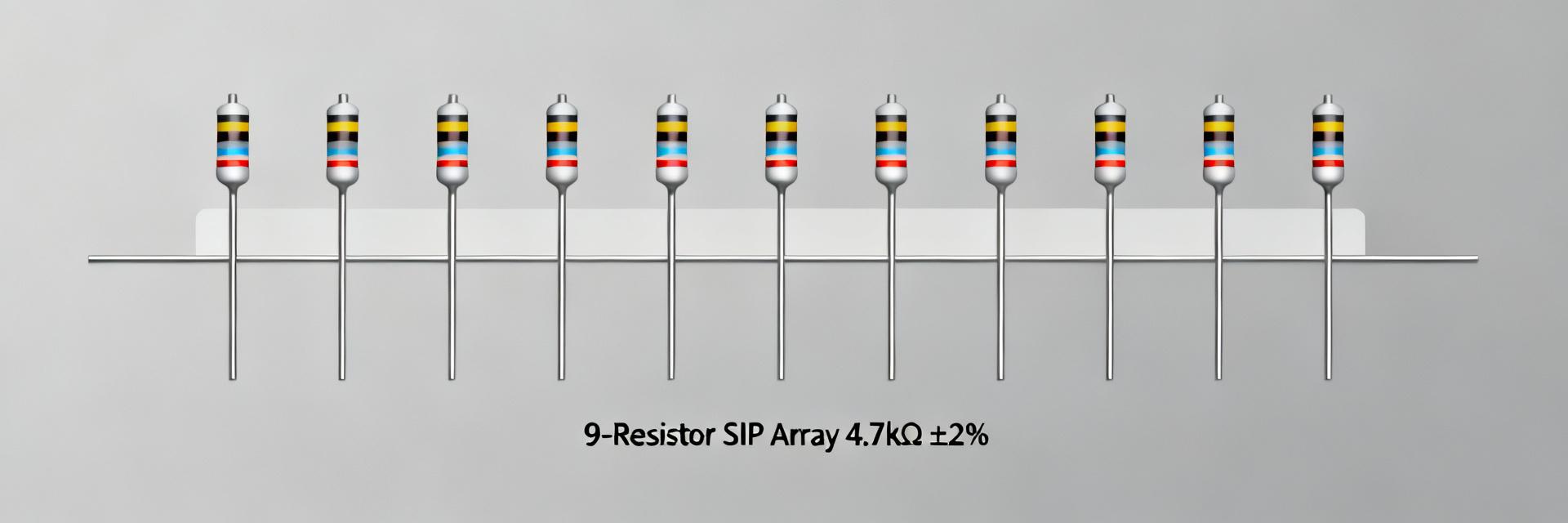
Point: The part number encodes topology, nominal value, and package family; MSP10A014K70GDA denotes a molded thick-film single‑in‑line 10‑pin package with nine resistor elements and a common bus.
Evidence: Datasheet block diagrams show a single common pin feeding nine individual resistors to the remaining pins.
Explanation: That bussed arrangement is ideal for pull networks and common reference returns but requires designers to plan for a single common node and to verify isolation to adjacent circuits.
Datasheet Sections to Extract
Point: A concise resistor array spec summary requires extracting specific datasheet tables: electrical characteristics, power‑vs‑temperature derating, mechanical drawing, and solder profile.
Evidence: The electrical table contains nominal resistance, tolerance, and TCR; power curves show per‑element derating with ambient temperature.
Explanation: Capturing those figures into the design repository shortens review cycles and ensures footprint and reliability checks are based on manufacturer test conditions rather than assumptions.
Electrical Specifications & Performance
Resistance, Tolerance and Temperature Coefficient
Point: Each element is nominally 4.7 kΩ with ±2% tolerance and a TCR on the order of 100 ppm/°C.
Evidence: The datasheet electrical table lists resistance, tolerance class, and typical TCR figures under specified test conditions.
Explanation: For voltage dividers and matched networks, ±2% and 100 ppm/°C imply potential ratio drift over temperature; designers should budget matching error and consider trimming or tighter components where necessary.
| Parameter | Value / Note |
|---|---|
| Nominal resistance | 4.7 kΩ per element |
| Tolerance | ±2% |
| TCR | ~100 ppm/°C (typical) |
| Power rating | 200 mW per element |
| Topology | 9‑resistor bussed, 10‑pin SIP |
Power Rating, Dissipation and Derating Calculations
Point: Rated at 200 mW per element, practical dissipation depends on ambient temperature and PCB thermal conductance.
Evidence: Power‑vs‑temperature derating curves in the datasheet define linear derating to 0 W at a maximum specified temperature.
Explanation: Use per‑element P = V²/R for steady‑state worst‑case; apply the derating factor from the datasheet for your board ambient to ensure element junction temperatures remain within limits.
Sample calculation: For a single element (4.7 kΩ) with 5 V across it, P = V²/R = 25 / 4700 ≈ 5.3 mW, well below 200 mW. Under PCB heating where derating reduces allowable power to 150 mW per element, this still provides a large safety margin for typical pull‑down use cases.
Thermal, Reliability & Environmental Data
Thermal Behavior & PCB Thermal Management
Point: Thermal path from chip to board is limited in a molded SIP; thermal resistance is nontrivial and PCB conduction matters.
Evidence: Mechanical and thermal notes recommend generous copper pads, stitched vias and minimal solder fillet shadowing to lower junction temperatures.
Explanation: Validate with IR imaging during a thermal soak at worst‑case power and use CFD or board‑level thermal simulation to size copper planes and via arrays that keep element temperature within derating limits.
Reliability Metrics & Environmental Compliance
Point: Key reliability tests are load life, humidity (damp heat), thermal shock and solderability; reports should list pass criteria and sample sizes.
Evidence: Datasheet reliability tables show test conditions and acceptance limits for resistance shift after stress.
Explanation: Summarize compliance (e.g., lead‑free solderability, RoHS/REACH statements if present) and include expected resistance shift margins in acceptance criteria for procurement and qualification.
Design Integration Guide
Footprint, Mechanical Constraints & Placement Tips
Point: A reliable footprint uses pads sized to match the molded leadframe, with controlled paste volume to avoid tombstoning and to ensure a consistent solder fillet.
Evidence: Mechanical drawing lists lead dimensions and recommended land pattern; recommended keepouts protect from flex and routing under the body.
Explanation: Orient the common bus pin consistently across the PCB, keep high‑stress routes clear of the package edge, and verify land pattern with a solderability run to ensure mechanical and electrical integrity after reflow.
Circuit-Level Usage & Worked Examples
Point: Common uses include pull networks and simple resistor ladders where identical values simplify layout.
Evidence: Using 4.7 kΩ elements in a divider yields predictable attenuation; numeric examples use Vdrop and P calculations from the electrical section.
Explanation: For a divider driven from 3.3 V, two series 4.7 kΩ yield midpoint V ≈ 1.65 V and per element dissipation ≈ 0.58 mW, making this array suitable when low power and matched values are acceptable.
Testing, Validation & Troubleshooting
Recommended Lab Tests & Measurement Setups
Point: Test sequence should include initial 4‑wire R measurement, power soak with temperature monitoring, and post‑stress resistance checks.
Evidence: Standard test methods call out durations (e.g., 1000‑hour load life) and resistance shift thresholds for acceptance.
Explanation: Use Kelvin probes to avoid lead resistance errors, log resistance vs. time during thermal soak, and set drift acceptance criteria consistent with design margin (for ±2% parts, a post‑test limit of ±4% might be used depending on application).
Common Failure Modes and Field Troubleshooting
Point: Typical field issues are solder fatigue, element opens, and drift from thermal overstress.
Evidence: Failure analysis of similar arrays often shows solder joint cracks or resistance shifts after repetitive thermal cycling.
Explanation: Troubleshoot by cross‑checking solder profiles, performing X‑ray or optical inspection, and if necessary redesigning the land pattern or adding conformal coating to mitigate moisture and mechanical stress.
Applications, BOM & Procurement Checklist
Typical Application Categories & Selection Criteria
Point: This 9‑element bussed SIP excels in pull/down arrays, reference networks and where board real estate is constrained.
Evidence: The combination of 4.7 kΩ, 200 mW rating and compact package matches many I/O pull‑networks and resistor‑ladder applications.
Explanation: Choose bussed arrays when a common node is required; pick isolated networks if individual isolation and higher power per element are needed.
BOM Attributes & Verification Checklist for Procurement
Point: The procurement checklist should lock down electrical, mechanical and verification attributes to avoid cross‑ship.
Evidence: BOM line item must reference part number, package drawing revision and required test reports.
Explanation: Require certificate of conformance and sample lot test reports during first purchase and maintain safety stock based on production cadence and lead time variability.
Summary
- The MSP10A014K70GDA resistor array (4.7 kΩ, ±2%, ~100 ppm/°C) requires designers to capture resistance, tolerance and TCR into tolerance budgets and matching analyses for divider accuracy and network symmetry.
- Thermal limits (200 mW per element with datasheet derating) drive PCB copper, via count and test validation; use thermal soak and IR imaging to confirm operating temperature under load.
- Footprint and soldering notes from the mechanical drawing plus a clear procurement checklist reduce assembly and field failures when verified by 4‑wire and load‑life testing.
FAQ
What are the key electrical limits of the MSP10A014K70GDA resistor array?
The primary electrical limits are 4.7 kΩ nominal per element, ±2% tolerance, ~100 ppm/°C TCR and 200 mW maximum dissipation per element before derating. Designers should reference the datasheet's power‑vs‑temperature curve and use P = V²/R to verify steady‑state dissipation against the derating line.
How should I calculate thermal derating for PCB mounting?
Use the datasheet derating curve to get the allowable power at your board ambient, then simulate or measure board temperature rise. Apply thermal simulation or IR imaging during a controlled soak, adjust copper planes/vias to lower junction temperature, and ensure per‑element dissipation stays beneath the derated limit.
Which lab tests are recommended to validate a resistor array spec?
Recommended tests include initial 4‑wire resistance measurement, thermal soak with power applied, load‑life (extended bias) and humidity/thermal shock. Define acceptance criteria based on allowable drift (e.g., a conservative multiple of original tolerance) and record sample sizes and test durations for qualification.
What are the common failure modes and field troubleshooting actions?
Typical field issues include solder fatigue (cracking under thermal cycling), element open circuits, and parametric resistance drift from thermal overstress. Corrective actions involve verification of reflow oven thermal profiles, optimization of PCB footprint pad dimensioning, and application of conformal coatings to guard against moisture and mechanical stress.