STGSH50M120D Datasheet Analysis: Key Electrical Specs & Design Tips
Struggling to decode the dense tables and graphs of power semiconductor datasheets? You are not alone. For engineers designing high-power inverters or servo drives, selecting the right module is critical, yet often hindered by complex parameter interpretation. This guide breaks down the STGSH50M120D datasheet into actionable insights, helping you navigate its 1200V half-bridge topology with confidence. By understanding its key electrical specs and thermal characteristics, you can optimize your design for efficiency and reliability in US market applications.

Decoding Core Electrical Specifications
To leverage the full potential of this IGBT module, you must first interpret its fundamental electrical parameters correctly. Misreading these values can lead to excessive heat generation or premature failure in demanding industrial environments.
Understanding VCE(sat) and Current Ratings at 1200V
The collector-emitter saturation voltage (VCE(sat)) is a primary driver of conduction losses. In the STGSH50M120D, this value typically hovers around 1.7V to 1.9V at nominal currents of 50A. However, note that VCE(sat) increases with junction temperature. Engineers should always check the curve at Tj = 150°C rather than just the 25°C typical value. A higher saturation voltage directly translates to more wasted energy as heat, reducing overall system efficiency. Ensure your cooling solution accounts for this worst-case scenario.
Analyzing Gate Charge Parameters for Switching Speed Optimization
Switching performance is governed by gate charge (Qg) and gate resistance (Rg). The total gate charge determines how much current your gate driver must supply to switch the device on and off. Lower Qg allows for faster switching speeds, which reduces switching losses but may increase electromagnetic interference (EMI). Conversely, slower switching minimizes EMI but raises thermal stress. Balancing these trade-offs requires careful selection of Rg. Typically, an Rg between 4.7Ω and 10Ω offers a robust compromise for most servo drive applications, ensuring clean waveforms without excessive ringing.
Thermal Management and Reliability Insights
Power electronics live and die by their thermal management. The physical packaging and internal material choices dictate how effectively heat escapes the silicon chip before it causes irreversible damage.
| Parameter | Symbol | Value / Condition |
|---|---|---|
| Max Junction Temperature | Tj,max | 150 °C |
| Thermal Resistance (J-C) | Rth,jc | Low (ACEPACK SMIT) |
| Short Circuit Withstand | tsc | ≥ 10 µs |
Junction Temperature Limits and Power Dissipation Calculations
The maximum junction temperature (Tj,max) for this component is strictly limited to 150°C. Exceeding this threshold even momentarily can degrade the oxide layers and shorten the lifespan significantly. To calculate actual power dissipation, use the formula P = VCE(sat) × IC for conduction losses, plus switching energy per cycle multiplied by frequency. Remember that the ACEPACK SMIT package has a specific thermal resistance from junction to case (Rth,jc). Your heatsink design must ensure that the temperature rise across this interface keeps Tj well below 150°C under peak load conditions.
Short-Circuit Ruggedness and Safe Operating Area (SOA) Guidelines
Industrial environments are prone to transient faults. The short-circuit withstand time is a critical metric for reliability. While specific values vary by operating point, generally, these modules support short-circuit durations of 10 microseconds or more when properly driven. Always refer to the Forward Bias Safe Operating Area (FBSOA) graph in the datasheet. This chart defines the limits of current and voltage combinations where the device remains safe during turn-on and turn-off transitions. Operating outside these boundaries risks latch-up or avalanche breakdown, leading to catastrophic failure.
Practical Design Tips for Circuit Integration
Translating theoretical specs into a working board requires attention to layout details. Small parasitic elements can drastically alter performance compared to ideal simulations.
Optimizing PCB Layout for Surface-Mount ACEPACK SMIT Packages
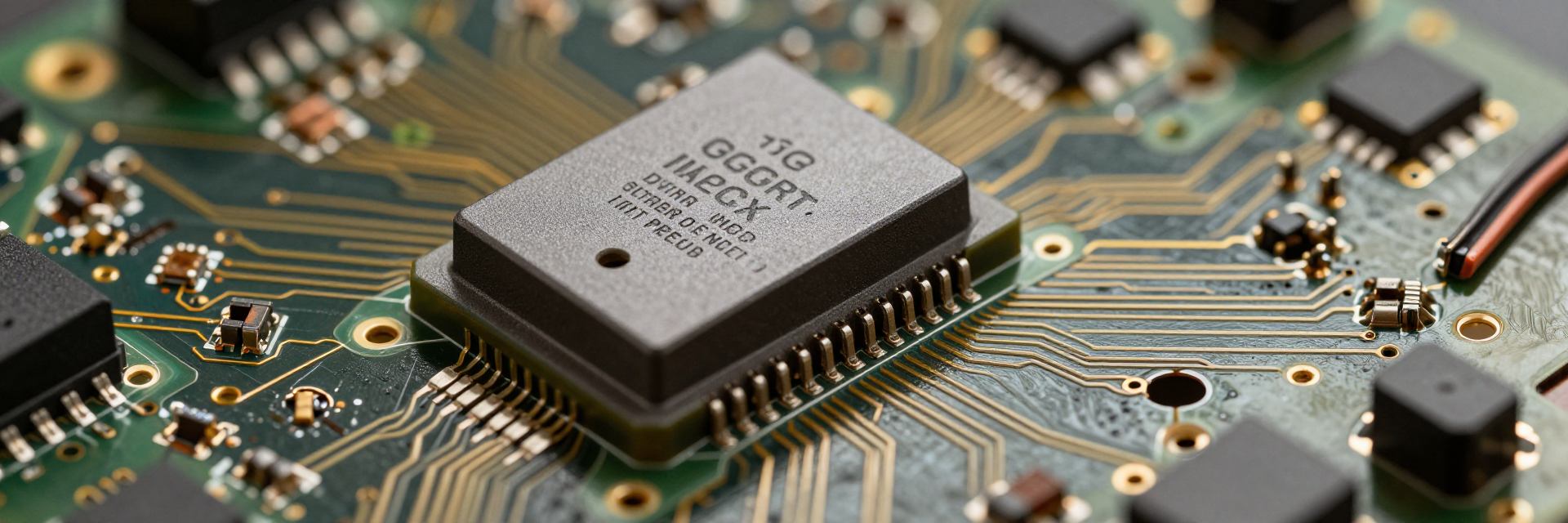
The surface-mount nature of the ACEPACK SMIT package demands precise solder paste application and reflow profiles. Keep commutation loops as short as possible to minimize parasitic inductance. High di/dt events generate significant voltage spikes across stray inductances (L × di/dt), which can exceed the breakdown voltage of the IGBT. Use wide copper traces for power paths and place decoupling capacitors directly adjacent to the DC bus terminals. Symmetrical routing for both switches in the half-bridge ensures balanced current sharing and prevents one side from overheating disproportionately.
Snubber Circuit Design to Mitigate Voltage Spikes
Even with optimized layouts, some voltage overshoot is inevitable due to inherent circuit inductance. Implementing a snubber network—typically a resistor-capacitor (RC) pair connected across the DC link or individual switches—can dampen these oscillations. Start with a small capacitor value, such as 10nF to 47nF, and adjust the resistor to critically damp the ringing without introducing excessive loss. Monitor the waveform using a differential probe during testing; if oscillations persist above 10% of the bus voltage, refine your snubber values. This step protects the gate oxide and improves EMC compliance.
Real-World Application Scenarios
Understanding where this component fits best helps avoid over-engineering or under-specifying your design. Its 1200V rating makes it suitable for three-phase systems up to approximately 800VDC bus voltage.
Implementation in Industrial Servo Drives and Inverters
In servo drives, dynamic response is crucial. The fast switching capabilities of the STGSH50M120D allow for higher PWM frequencies, resulting in smoother motor control and reduced acoustic noise. For general-purpose inverters, its robustness against overload conditions provides a safety margin during startup surges. Many designers choose this module for mid-power applications ranging from 15kW to 30kW, where discrete solutions become too bulky and larger modules are cost-prohibitive. Its integrated diodes simplify the schematic, reducing bill-of-materials complexity.
Comparison with Alternative IGBT Modules for Cost-Performance Balance
When comparing alternatives, consider not just the unit price but the total system cost. Some competitors offer lower VCE(sat), which saves energy but may require more expensive gate drivers or larger heatsinks. Others might have higher ruggedness but slower switching speeds. Evaluate your priority: if efficiency is paramount for long-running pumps, prioritize low conduction losses. If space is constrained in compact robotics, favor smaller footprints like the ACEPACK series. Always run a thermal simulation for each candidate to verify they meet your ambient temperature requirements without derating excessively.
Key Takeaways
- Thermal Limits: Strictly maintain junction temperatures below 150°C by accounting for VCE(sat) increases at high temperatures.
- Layout Precision: Minimize commutation loop inductance in PCB design to prevent destructive voltage spikes during switching.
- Gate Drive Tuning: Optimize gate resistance to balance switching speed against EMI and thermal stress.
- Application Fit: Ideal for 15-30kW servo drives and inverters requiring a compact, integrated half-bridge solution.
Frequently Asked Questions
What is the maximum current rating for the STGSH50M120D?
The nominal continuous collector current is rated at 50A. However, this value depends heavily on the case temperature and duty cycle. Always consult the derating curves in the datasheet to determine the safe operating current for your specific thermal environment, as exceeding this limit will cause rapid overheating.
How does the ACEPACK SMIT package affect thermal performance?
The surface-mount ACEPACK SMIT package offers low thermal resistance from junction to case, facilitating efficient heat transfer to the PCB or baseplate. It eliminates the need for mechanical mounting hardware, reducing assembly costs while maintaining reliable thermal contact through solder joints and appropriate pad design.
Can this module be used in parallel configurations?
Yes, multiple units can be paralleled to handle higher currents, but this requires careful balancing. Match gate resistors closely and ensure symmetrical PCB layouts to guarantee equal current sharing among devices. Without proper balancing, one module may carry disproportionate load, leading to uneven heating and potential failure.
What is the recommended gate resistance range?
Typically, an Rg between 4.7Ω and 10Ω offers a robust compromise for most servo drive applications, ensuring clean waveforms without excessive ringing or EMI issues.