MPMT1002BTS Specs Report: Precise Resistor Network Data
Precision resistor arrays used as matched divider elements directly set ADC accuracy, offset and drift in bias networks. Typical measured/typical specs for the device addressed here include matched 5 kΩ / 5 kΩ elements, ±0.1% absolute resistance tolerance, 100 mW power per element and tight inter-element tracking on the order of tens of ppm/°C. This report gives a clear, testable specs overview, interpretation guidance and an actionable checklist engineers can use when evaluating this resistor network in precision divider and ADC front-end applications. The goal is a concise, laboratory-oriented reference for verification and procurement decisions.
1 — MPMT1002BTS: package, pinout and basic spec summary (background)
1.1 Electrical core specs
Point: Core electrical parameters determine whether the part meets system error budget. Evidence: Report these nominal table-ready values for copy into BOM and test plans. Explanation: Use the following exact spec set when comparing parts in qualification: nominal element value 5 kΩ each; absolute tolerance ±0.1%; element configuration matched pair (divider topology); power per element 100 mW continuous; maximum working voltage 100 V; typical tracking/TCR figures ~25 ppm/°C (typical) with worst-case published limits higher. Treat values labeled “typical” as expected central tendency and “maximum” as guaranteed limits in datasheet verification.
1.2 Physical package & pinout essentials
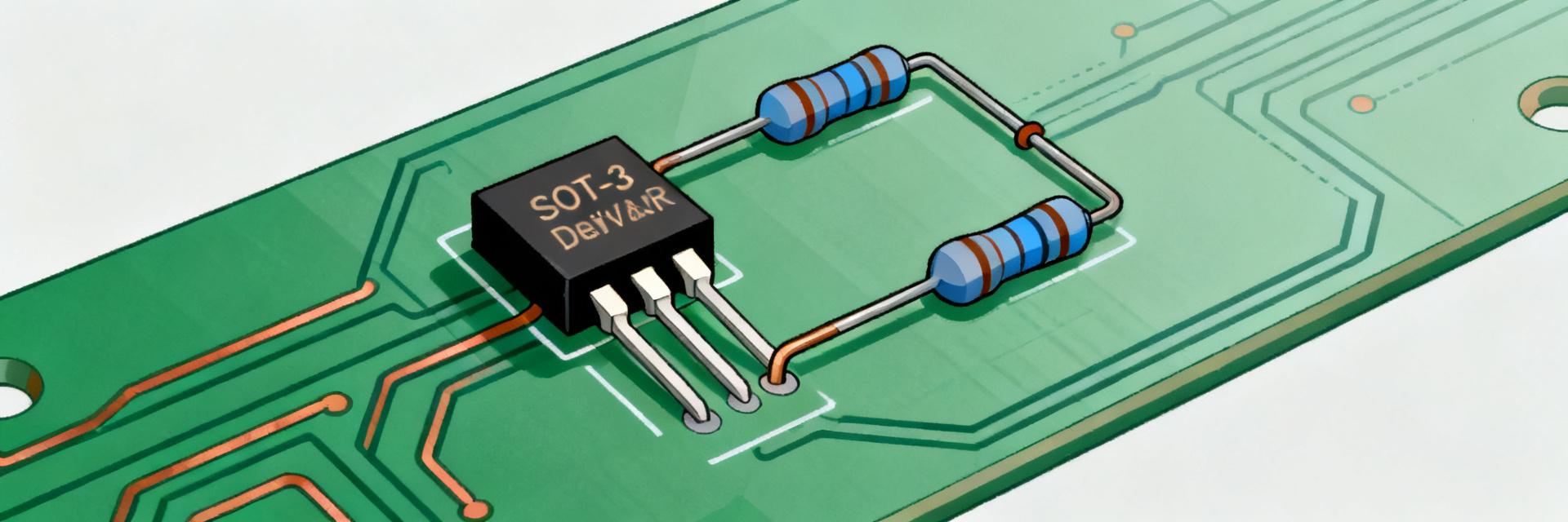
Point: Mechanical footprint and thermal path affect real-world dissipation and assembly yield. Evidence: Verify package type, pad pitch, max seated height and pin numbering against PCB artwork. Explanation: Check orientation notch or marking for correct rotation; confirm pad pitch and copper land pattern matches manufacturer footprint. Note maximum seated height for enclosure constraints and consider thermal relief copper area under each resistor to improve continuous power capability. Quick visual checks on incoming reels should include marking legibility and consistent lot codes for traceability.
2 — Electrical characteristics deep dive: resistance, tolerance and tracking
2.1 Resistance values, tolerance and ratio accuracy
Point: Absolute resistance and ratio error define divider accuracy before calibration. Evidence: With ±0.1% absolute tolerance, ratio tolerance can be much tighter depending on element matching and process controls. Explanation: For a two-element divider with R1 and R2 nominally 5 kΩ, absolute tolerance ±0.1% yields possible single-element variation of ±5 Ω. Ratio error (ΔR/R) between elements governs divider output error; if matching process yields ratio tolerance near 0.05–0.1% the uncalibrated divider error reduces accordingly. Use divider output error ≈ (R2/(R1+R2))·(ΔR/R) to estimate offset into an ADC; for a 1:1 divider any mismatch directly maps to half-scale offset in relative terms. When tight ratio is required, specify ratio tolerance and include ratio screening in incoming inspection for production builds. The term resistor network is central here because matched elements within the same package typically show superior ratio stability versus discrete parts.
2.2 TCR, tracking and temperature behavior
Point: Temperature coefficient and inter-element tracking determine temperature-induced drift of divider outputs. Evidence: Typical TCR numbers are tens of ppm/°C; tracking between elements is the critical metric for divider stability. Explanation: Define TCR as ΔR/R per °C and tracking as differential Δ(TCR) between elements. If nominal TCR = 50 ppm/°C and tracking = 25 ppm/°C, a 40 °C swing yields ~2 ppm relative shift in ratio for well-tracked elements, substantially smaller than absolute change. For systems sensitive to thermal transients, specify tracking (ppm/°C) rather than only absolute TCR, and consider temperature compensation or on-board calibration if worst-case envelope might exceed error budget. Report both typical and worst-case scenarios in qualification reports.
3 — Power, voltage limits and reliability metrics
3.1 Power dissipation and derating
Point: Per-element power limits plus PCB thermal design determine safe continuous operation. Evidence: With 100 mW rated per element, calculate dissipation from applied voltage and compare to derated limits at ambient. Explanation and worked example: For a 5 kΩ resistor, V across resistor that produces 100 mW is V = sqrt(P·R) = sqrt(0.1 W·5,000 Ω) ≈ 22.36 V. Continuous operation at 20 V yields P = V^2/R = 400/5000 = 0.08 W (80 mW), within rating. If the board copper area under the part is reduced, derating curve applies — reduce allowable continuous power by the datasheet derating factor for the expected ambient. For pulsed loads, compute energy per pulse and ensure thermal time constants prevent overheating.
3.2 Voltage rating, stability and long-term drift
Point: Maximum working voltage and environmental stresses influence long-term ppm/year drift. Evidence: Use maximum working voltage (e.g., 100 V) as primary constraint; humidity, temperature cycling and DC bias stress accelerate drift. Explanation: For high-voltage applications, derate if combined power and voltage produce elevated surface fields. Recommend accelerated load-life tests (biased at elevated temperature and humidity) to quantify ppm/year drift for system reliability targets. Document lot-level drift statistics and include periodic requalification when sourcing changes occur.
4 — Measurement & test methods to validate MPMT1002BTS specs
4.1 Recommended bench tests and instrumentation
Point: Proper instrumentation and methods are essential to validate tight ratio and TCR numbers. Evidence: Use four-wire precision ohmmeters, bridge instruments and temperature chambers for controlled tracking tests. Explanation: For ratio checks aim for micro-ohm or sub-ppm resolution depending on expected matching; use four-wire Kelvin connections to eliminate lead resistance. Perform matched temperature chamber sweeps to quantify tracking (ppm/°C) and repeat measurements at multiple lot samples. Avoid measurement artifacts by stabilizing thermal gradients, using low-EMF connectors and allowing adequate settling after power application.
4.2 Interpreting datasheet data vs. lab results
Point: “Typical” datasheet numbers represent central tendency; qualification requires comparing to guaranteed limits. Evidence: Establish pass/fail thresholds based on application error budget and statistical sampling. Explanation: Use a sampling plan (e.g., MIL/IPC-style) with acceptance criteria tied to absolute and ratio tolerances; if measured population mean or sigma exceeds datasheet typical behavior, consider batch re-screening. For marginal parts, define rework or calibration steps and include lot traceability in procurement records.
5 — Implementation checklist and procurement/qualification notes
5.1 Quick spec verification checklist
Point: A concise incoming-inspection checklist saves qualification time and prevents field failures. Evidence: Verify key electrical and mechanical items on receipt. Explanation: Minimum incoming checks: confirm nominal resistance & ratio, absolute tolerance ±0.1% verification, TCR/tracking spot check, power and voltage rating verification, and package/pinout marking and lot traceability. Define acceptance criteria numerically (e.g., ratio within 0.05% for critical lots) and include remedial steps: full 100% sort, sample-based screening, or order return for out-of-spec lots.
5.2 Replacement, equivalents and sourcing considerations
Point: When substituting, match electrical configuration and thermal behavior, not just nominal resistance. Evidence: Key matching parameters are element configuration, tolerance, TCR/tracking and power rating. Explanation: Document substitutions with formal qualification tests: ratio checks, thermal cycling and load-life tests in-system. Maintain a substitution matrix in procurement records showing tested equivalence criteria and system-level performance verification steps to ensure no regression in ADC offset, gain or long-term drift.
Summary
Recap: Core numeric specs to capture in design and procurement are: nominal 5 kΩ elements, ±0.1% absolute tolerance, per-element power 100 mW, maximum working voltage ~100 V and typical tracking figures on the order of tens of ppm/°C. The most critical validation steps are four-wire ratio checks, temperature chamber tracking tests and power/voltage derating calculations. Practical PCB/thermal checks include copper area under the part and correct pad/pitch matching during footprint review. MPMT1002BTS should be specified with both typical and maximum datasheet values recorded in the test plan; include lot traceability and documented acceptance criteria. Consider adding a one-row BOM spec table and a simple measurement worksheet to the engineering spec sheet to improve usability and shareability.
| Parameter | Value |
|---|---|
| Nominal resistance (per element) | 5 kΩ |
| Absolute tolerance | ±0.1% |
| Configuration | Matched pair (divider) |
| Power per element | 100 mW |
| Max working voltage | 100 V |
| TCR / Tracking (typical) | ~25 ppm/°C (tracking) |
| Package notes | Check pad pitch, orientation marking, seated height |
Technical FAQs
What is the ratio tracking specification of the MPMT1002BTS?
The typical tracking TCR is on the order of tens of ppm/°C (typically ~25 ppm/°C), which ensures ratio stability over temperature swings.
How does absolute tolerance affect ratio accuracy in the divider?
While absolute tolerance is ±0.1% (yielding up to ±5 Ω variation on each 5 kΩ element), the ratio tolerance is typically much tighter due to matched inter-element fabrication.
What is the maximum continuous power rating for each resistor element?
Each element is rated for up to 100 mW continuous power, subject to derating curves at elevated ambient temperatures.
Which measurement technique is recommended to validate the divider ratio?
A four-wire Kelvin connection and high-precision ohmmeters are recommended to eliminate test lead resistance artifacts during testing.