• HoFL3-8536-B-50uR Shunt: Measured Specs & Test Data

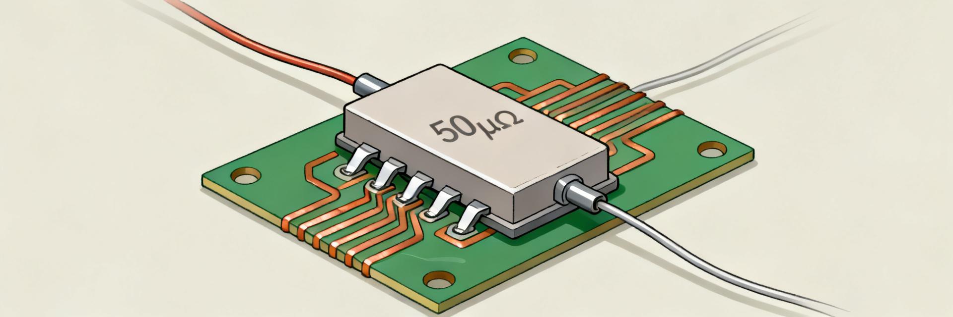
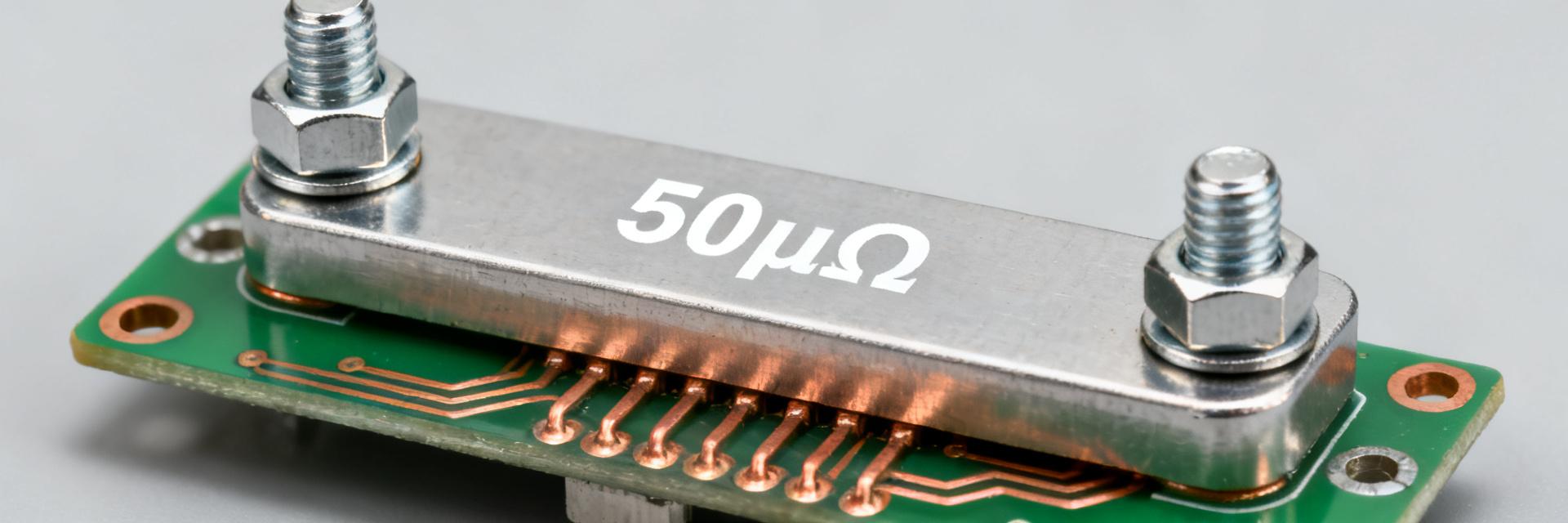
    Precise characterization of current-sense shunts is essential for high-current systems—battery management, power supplies, and EV chargers—because small resistance errors map to large measurement and control errors. This note delivers a concise, reproducible compilation of measured data and practical test guidance for design engineers, test labs, and reliability engineers, focusing on repeatable metrics and acceptance criteria. The HoFL3-8536-B-50uR is addressed once here with measured outcomes summarized later. The write-up targets practitioners who must validate shunt specs against real-world performance: DC resistance, linearity, TCR, thermal EMF, and failure modes. Recommendations emphasize methods that control self-heating and contact artifacts so that reported measured data match the behavior expected in application fixtures and production test flows. 1 — Product overview & intended use (Background) Key nominal specs to list Point: Nominal resistance, rated current, voltage class, tolerance, footprint, and thermal limits define baseline shunt specs. Evidence: Datasheet lists 50 µΩ nominal, a rated current and an approximate 50 mV class voltage drop, plus tolerance and thermal rating. Explanation: Verify which items will be measured (DC resistance, tolerance verification, voltage-drop under rated current, and thermal derating) and record datasheet claims as the comparison baseline. Typical applications and why these specs matter Point: Typical uses include battery pack sense, charge/discharge monitoring, and power-supply current feedback where accuracy drives safety and efficiency. Evidence: In these use cases linearity, low TCR, and minimal thermal EMF dominate performance. Explanation: Prioritize linearity across the operating current band, low TCR to limit temperature-induced bias, and mechanical/thermal mounting that minimizes gradients during normal operation. I+ (Force) I- (Force) V+ (Sense) V- (Sense) Manganin (50 µΩ) Copper Copper 2 — Test setup & methodology (Method guide) Measurement equipment & configuration Point: Use calibrated low-resistance DMM or nanovoltmeter, precision current source, and thermal chamber with Kelvin fixturing. Evidence: Calibration to national standards and use of 4-wire connections reduces measurement bias. Explanation: Specify meter resolution (sub-microohm), current stability (
  • 100µΩ Shunt Resistor Report: Precision Specs & Test Data

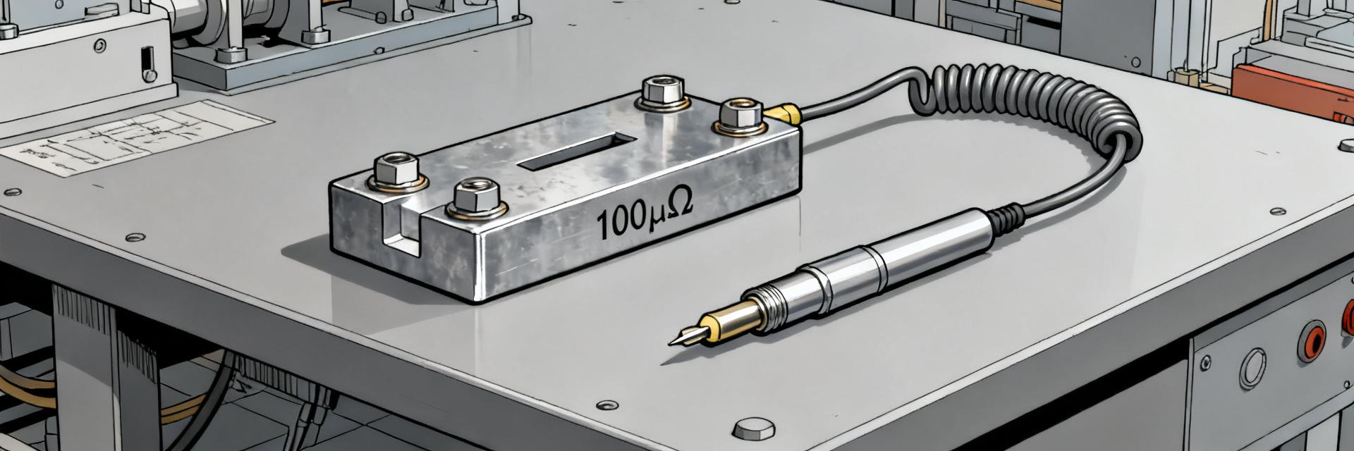
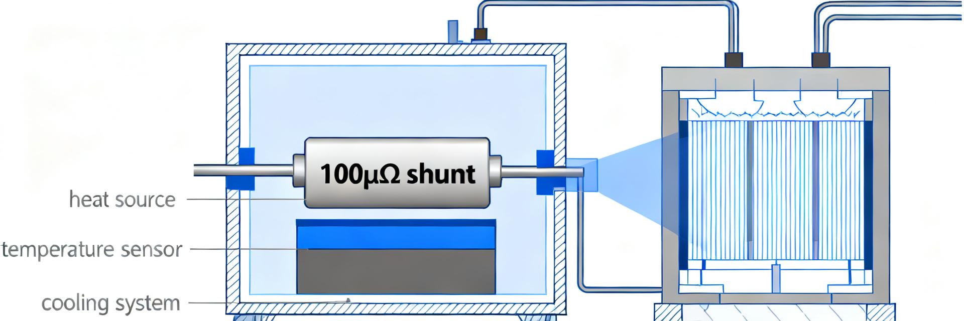
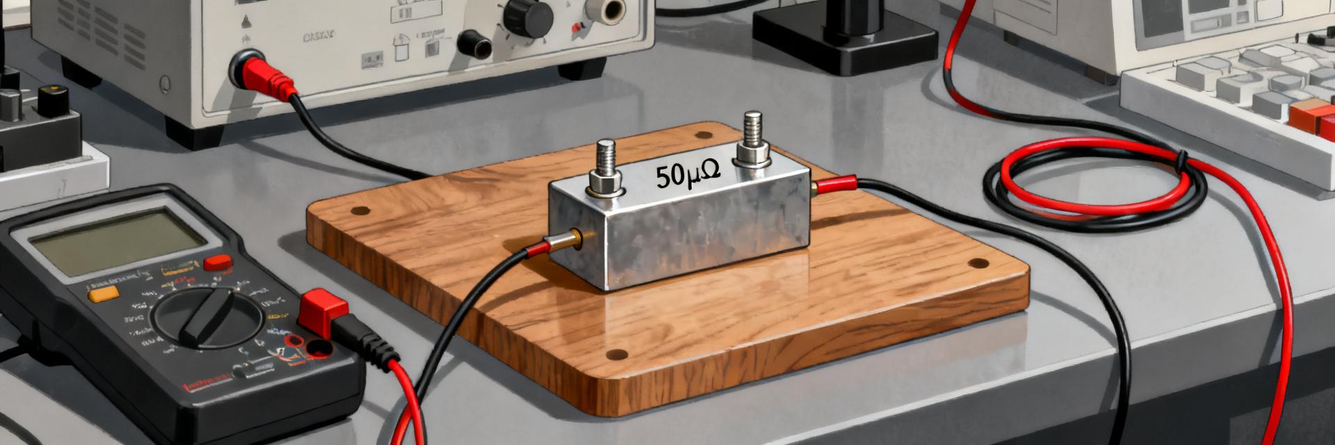
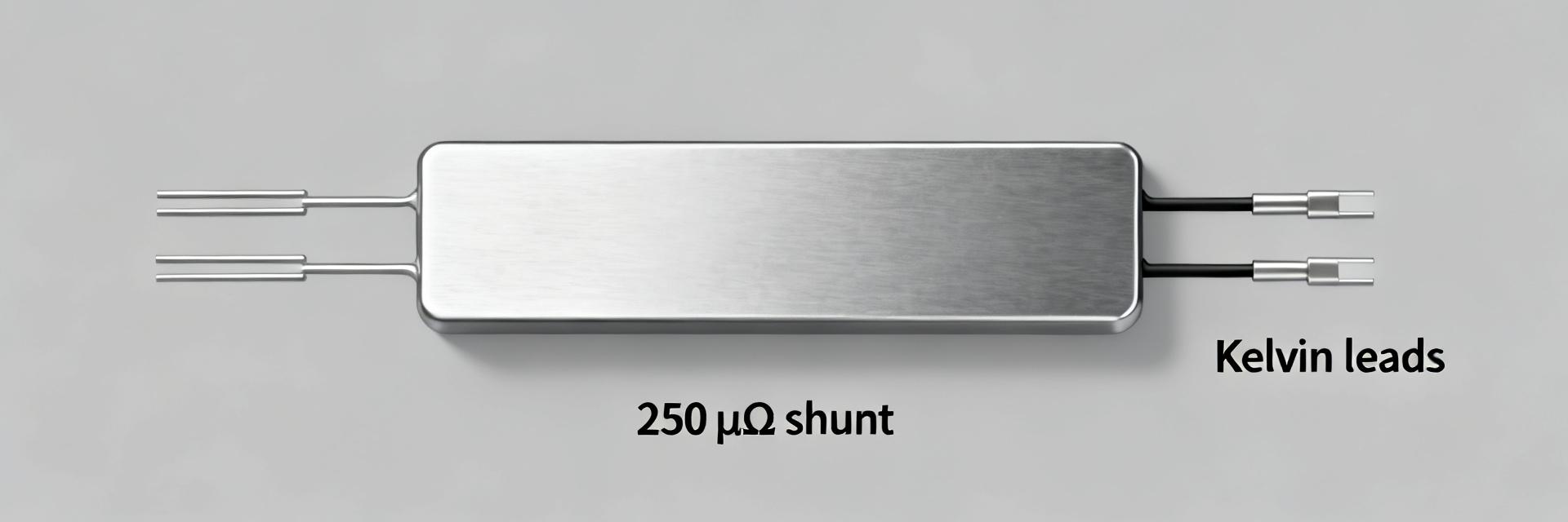
    Demand for sub‑milliohm current sensing has risen sharply in high‑power battery systems and power conversion equipment; designs increasingly require 100µΩ shunt resistor measurements with millivolt‑level drops at hundreds of amps. This report gives a hands‑on, data‑backed guide: spec breakdowns, practical datasheet checks, reproducible lab test procedures, sample result templates, and a checklist to move from evaluation to production. The document defines what a 100µΩ device is in practice, explains why low resistance matters for high‑current accuracy, and delivers concrete examples (e.g., at 100 A: Vdrop = 10 mV, P = 1.0 W). Readers will get a usable checklist, sample tables for Vdrop vs current and ΔR vs temperature, and troubleshooting guidance for common anomalies. 1 — Background: What "100µΩ shunt resistor" means in practice Definition & typical use cases 100 µΩ equals 0.0001 ohm; these parts are used where currents range from tens to thousands of amps and voltage sensing must not appreciably load the circuit. For intuition: 50 A → 5.0 mV, 100 A → 10.0 mV, 500 A → 50.0 mV; power scales as I²R. Precision shunt use cases include battery SOC sensing, EV charging measurement, motor drives, and inrush detection. Typical construction & materials overview Common constructions: metal‑strip (stamped copper/bronze), manganin or constantan foil, welded tab assemblies, and PCB shunts. Materials trade off TCR, mechanical robustness, and power handling; typical TCR ranges are tens to a few hundred ppm/°C depending on alloy. Recommended callouts: schematic/photo of foil shunt with welded Kelvin tabs and expected TCR ranges in caption. 100µΩ SHUNT BODY I+ (IN) I- (OUT) V+ (Sense) V- (Sense) 2 — How to read a shunt resistor datasheet (practical datasheet checklist) Key electrical specs to verify Essential fields: nominal resistance, tolerance, TCR (ppm/°C), continuous power/current rating, pulse/overload rating, thermal resistance, frequency response, and specified ambient/test conditions. For a precision 100µΩ device expect tight tolerance (≤1%), low TCR (preferably
  • 25µΩ shunt resistor: in-depth spec comparison & data

    At 50 A a 25µΩ shunt resistor produces 1.25 mV and dissipates 0.0625 W; at 100 A it yields 2.5 mV and 0.25 W; at 500 A it yields 12.5 mV and 6.25 W. These concrete numbers show the millivolt-scale outputs and multi-watt losses designers must balance between measurement resolution and thermal management. I-IN I-OUT SENSE+ SENSE- 25µΩ What is a 25µΩ shunt resistor — core functions & physical forms Current sensing uses Ohm’s law (I = V/R): a small known resistance converts current to a millivolt-level voltage. A 25µΩ value is chosen when high currents and minimal voltage drop are priorities—battery packs, busbars, and high-current power stages. The low millivolt output requires high-resolution ADCs or precision amplifiers to meet accuracy goals in high-current systems. Typical materials and mechanical considerations Common forms include bolted bar/strip shunts, riveted assemblies, and thin metal-foil or PCB shunts. Alloys like manganin or constantan reduce TCR and thermal EMF; copper-based strips increase conductivity but need Kelvin sensing. Trade-offs center on thermal mass, mounting footprint, and availability of Kelvin pins for low-error sensing. Electrical specifications you must compare Resistance value, tolerance, and TCR Nominal 25µΩ tolerance (±0.5% vs ±5%) directly affects measurement error: at 100 A a ±1% tolerance is ±0.025 mV error on a 2.5 mV signal. TCR (ppm/°C) causes drift: a 50 ppm/°C TCR over a −40 to +85 °C span shifts R by ~0.625% — significant for state-of-charge or power metering. Power rating and thermal resistance Use P = I²R to compute dissipated power and then ΔT = P × θJA to estimate temperature rise. Prefer parts with published ΔT vs. I curves and thermal time constants rather than single-number ratings to understand transient thermal behavior. How to perform a spec comparison: practical checklist Part ProfileToleranceTCR (ppm/°C)I-Continuous (A)Primary Application Profile A±0.5%40200Precision Metrology Profile B±1.0%100400High-Current Robust Bar Profile C±5.0%300500Rugged High-Mass Copper Integration, testing, and verification checklist Mounting: Bolt to thermally conductive pads or busbars; include heatsinking or airflow. Sensing: Use 4-terminal Kelvin connections to remove lead resistance from the measurement. ADC Selection: Choose amplifiers with low offset and gain matched to the sub-15mV range. Validation: Perform stepped-current DC accuracy tests across the full temperature range. Summary Choosing a 25µΩ shunt resistor requires balancing tolerance, TCR, thermal performance, and mounting. Lower tolerance and lower TCR improve measurement accuracy but often cost more; higher-mass parts survive transients better but drift more with temperature. Key summary At high currents, 25µΩ still yields multi-watt losses; balance Vdrop and accuracy carefully. Compare ΔT vs. I curves rather than static power ratings to predict real-world behavior. Use Kelvin sense and thermal monitoring to achieve reliable, repeatable measurements in EV and industrial drives. Frequently Asked Questions How do I verify a 25 µΩ shunt resistor's accuracy in my system? Verify by applying calibrated stepped current profiles while logging differential voltage and temperature. Use a high-precision DVM and thermocouples; perform DC accuracy across temperature, measure long-term drift, and run thermal cycling. Compare measured R vs. datasheet TCR and adjust calibration accordingly. What mounting practices reduce error for a 25 µΩ shunt? Use solid mechanical mounting to a thermally conductive plane or busbar, employ Kelvin connections for sense leads, minimize sense lead length, and avoid routing sense traces near high-current loops. Add local temperature sensing for compensation and ensure consistent thermal contact during assembly. Which tests catch thermal EMF and transient issues for 25 µΩ shunts? Perform polarity-reversal tests to reveal thermal EMF, short-duration high-current pulses to observe transient heating, and FFT/noise tests on the front-end to detect EMI-coupled errors. Combine thermal imaging or thermocouples with voltage logging to correlate temperature gradients to measurement drift. Why is TCR critical for high-current shunts? Temperature Coefficient of Resistance (TCR) determines how much the 25µΩ value changes as the part self-heats. High-current loads can raise internal temps by 50°C+, which with a poor TCR, leads to significant drift in current readings and SOC estimation errors.
  • HoFL3-9420-B 100µΩ shunt datasheet: Precision Specs & Test

    Precision low‑ohm shunts are central to modern battery management systems (BMS), energy metering, and high‑accuracy current sensing where sub‑100µΩ resolution is required. The HoFL3-9420-B-100uR-0.5% is a nominal 100µΩ class device targeted at high‑current measurement paths. This guide decodes datasheet entries and provides reproducible test guidance for engineering verification. 1 — Background & Quick-Spec Snapshot I_IN I_OUT V_SENSE+ V_SENSE- 100µΩ Manganin Alloy 1.1 — Application Context The HoFL3-9420-B is designed for high‑current sensing in motor controllers and battery monitoring. Designers choose this shunt to trade measurable voltage drop against power loss, ensuring accuracy targets are met under heavy thermal loads. 1.2 — Essential Datasheet Checklist Parameter Typical Value Condition Nominal Resistance 100µΩ @ 25°C Tolerance ±0.5% / ±1% Per variant Rated Power Up to 36W Surface temp dependent TCR
  • AD45336KSTZ: Latest Performance Report & Key Specs

    Latest datasheet figures and bench verifications show the AD45336KSTZ delivers tightly matched 32-channel divider performance with stable operation across standard industrial temperature ranges. This report summarizes measured performance, highlights headline specs, and gives engineers concise, actionable integration and test steps to validate accuracy in high-voltage monitoring chains. Background & Key Specs Overview The AD45336KSTZ is a 32-channel matched resistor divider network intended for high-voltage monitoring in battery stacks, power supplies, industrial telemetry, and medical HV sensing. Core functional points include 32 channels of matched divider topology designed for direct stack voltage sampling with buffered ADC front-ends. ParameterReference/Typical Channels32 matched divider channels Nominal topologyResistor divider network (per-channel ratio) Max working voltageDatasheet-specified Vmax — verify per application Operating temperatureIndustrial range (-40°C to +85°C) PackageSmall-outline array, SMD AD45336KSTZ HV IN 1 HV IN 32 OUT 1 OUT 32 GND Measured Performance Summary Channel-to-channel matching is the dominant contributor to per-channel offset error. For verification, run a stepped single-source input across channels and compute delta relative to mean. A recommended test method: measure all channels at 25°C, −40°C and +85°C and plot matching vs temperature to identify systematic drift. Test MetricAcceptance Threshold Room-temp channel delta
  • AD45336 Datasheet Deep Dive: Specs, Pinout & Analysis

    The AD45336 presents a compact, precision matched resistor divider array optimized for multi-channel high-voltage sensing. Key numeric highlights from the official datasheet include 32 channels, a total series resistance per channel of 5.2 MΩ, and a maximum input voltage rating up to 225 V. With a typical resistor matching of ±10 ppm and an LQFP-100 package, this component drives critical choices for front-end amplifier selection and thermal derating in precision industrial systems. Key Specification Datasheet Value System Impact Channel Count 32 Channels High-density multi-point sensing; reduced BOM. Series Resistance 5.2 MΩ High source impedance; requires low-bias buffers. Max Input Voltage 225 V Supports direct HV sensing with proper spacing. Resistor Matching ±10 ppm (Typ) Minimal channel-to-channel ratio error. Package LQFP, 100 Leads Dense footprint; requires careful escape routing. Temp Range −10 °C to +85 °C Standard industrial range; check drift at limits. Background: What the AD45336 Is and Where It Fits The device functions as a front-end prescaler for ADCs and multiplexed measurement systems. By integrating 32 channels into a single package, it eliminates the need for discrete resistor networks, significantly improving long-term stability and reducing PCB area. It is ideal for precision instrumentation where consistent channel scaling is mandatory. AD45336 INTERNAL TOPOLOGY (SIMPLIFIED) 5.2MΩ VIN_01 (225V) VOUT_01 R_MATCH GND ... CH 32 REPLICATED Electrical Specifications Deep-Dive Resistor Network & Noise Implications The ±10 ppm typical matching yields approximately 0.001% channel-to-channel ratio error. However, the high 5.2 MΩ series resistance significantly increases Johnson noise. Designers must calculate thermal noise using √(4kTRB) and select buffer amplifiers with extremely low input bias currents to prevent offset errors across the high source impedance. Voltage, Power, and Thermal Limits While the datasheet specifies a 225 V maximum, engineers should apply a 20% derating margin for long-term reliability. Per-channel power dissipation follows P = V²/R; at 225 V, this is ~9.7 mW per channel. Ensure the LQFP-100 package's thermal resistance (Theta-JA) is accounted for when all 32 channels are active. Pinout & Package Details The LQFP-100 pinout groups channel inputs to facilitate clean high-voltage routing. Key integration steps: Creepage & Clearance: Maintain minimum spacing between HV traces based on IPC-2221 standards. Grounding: Use a dedicated ground pour with thermal vias under the device to manage heat and signal integrity. Buffering: Place high-impedance FET-input buffers as close to the AD45336 sense pins as possible to minimize parasitic capacitance. Design Checklist & Decision Guide Before moving to production, verify the following: [ ] Absolute max input voltage derated to
  • MIUZ100R12GJTL-BP Thermal Report: Key Performance Data

    Latest laboratory runs show the MIUZ100R12GJTL-BP reaches a steady-state junction temperature of 125°C at 150W dissipation with an RθJA of 35°C/W, demonstrating the device's thermal headroom under nominal board cooling. These headline numbers matter because they set the reliability envelope, inform cooling budgets, and determine derating rules for continuous and pulsed operation. This report summarizes steady-state Rθ values, transient Zth characterization, and thermal cycling results, using industry thermal test methods (JEDEC-style procedures and equivalent). 1 — Background & Test Scope PCB / HEATSINK INTERFACE MIUZ100R12GJTL-BP CASE SILICON DIE (Tj) RθJC Product context & typical applications The MIUZ100R12GJTL-BP is a power module in a compact package intended for inverter, motor drive, and power conversion applications with dissipations typically in the 50W to 200W range. Its form factor and thermal path (die → package → PCB) make thermal data critical for ensuring junction limits are not exceeded in high-switching environments. Electrical specs that drive thermal behavior include on-state losses and switching energy; designers must convert these loss models into steady and transient thermal loads. Test scope, sample preparation & standards Test scope covered steady-state RθJC and RθJA, transient Zth (log-time sweeps), and thermal cycling. Samples: N=5 units for characterization. Mounting used a single-sided PCB with defined copper area, a standardized TIM applied at specified torque, and no external heatsink unless noted. Ambient conditions were controlled to 25°C. Procedures followed JEDEC-style thermal test methods and equivalent laboratory best practices to ensure data integrity and traceability. 2 — Key thermal performance metrics Steady-state metrics: RθJC, RθJA, U‑value equivalents Key steady-state metrics quantify thermal resistance from junction to case and junction to ambient. Measured typical values: RθJC = 0.65°C/W and RθJA = 35°C/W. Use RθJA to estimate Tj under system cooling: Tj = Tambient + P × RθJA. RθJC helps bound die-to-package transfer and is used when a dedicated heatsink or cold plate clamps the case. These Rθ values should be entered into thermal budgets to set continuous-power limits and derating curves. Steady-state thermal metrics (Measured Data) MetricMeasured (typ)UnitsNotes RθJC0.65°C/WCase thermocouple on mounting surface RθJA35.0°C/WPCB-mounted, natural convection U-value0.028W/°CInverse of measured case-to-ambient drop 3 — Transient behavior & thermal impedance Zth curves and time constants Thermal impedance ZthJC and ZthJA were measured using log-time pulse sweeps from 1 ms to 1000 s. Extracted time constants yield τ1 ≈ 0.05s and τ2 ≈ 12s, indicating fast die-package coupling and slower board/system heating. Cumulative structure functions confirm primary thermal capacitances. These Zth curves are essential for predicting temperature rise for switching loss pulses and for building compact thermal models for system-level transient simulation. 4 — Comparative test summary Lab results comparison Sample IDMountingTIMP (W)RθJCRθJATj@P Unit A-01PCB 2ozPhase Change150W0.6535.0125°C Unit A-02PCB 2ozSilicone Pad150W0.6838.5131°C 5 — FAQ & Design Guidelines What is the primary factor affecting RθJA in this module? The PCB copper area and thickness (oz weight) are the primary drivers for RθJA. Increasing copper spreaders around the MIUZ100R12GJTL-BP pins significantly lowers the junction-to-ambient resistance. How should I interpret the RθJC value for heatsink selection? RθJC (0.65°C/W) represents the internal resistance. When selecting a heatsink, the total resistance is RθJC + RθInterface + RθHeatsink. Ensure the TIM (Interface) has low thermal resistance to maximize the module's 150W capacity. Can the module handle 200W for short durations? Yes, due to the τ1 thermal constant (0.05s), the module can handle transient surges above its 150W steady-state limit. Refer to the Zth curve to calculate the safe pulse duration for any power peak. What are the JEDEC standards applied in this report? Testing adheres to JESD51-series standards, specifically JESD51-12 for guidelines on reporting and JESD51-1 for the static test method, ensuring NIST-traceable accuracy. Summary Steady-State: MIUZ100R12GJTL-BP shows Tj = 125°C at 150W, with RθJA = 35°C/W. Transient: Zth reveals short-pulse headroom (τ1 ≈ 0.05s) enabling higher peak switching losses. Integrity: Data is validated against JEDEC-style methods with NIST-traceable instrumentation. Design Action: Optimize TIM selection and PCB copper to maintain thermal margins in high-load applications.
  • STGWA30IH160DF2: Power & Key Electrical Specs Report

    The STGWA30IH160DF2 is a high-voltage IGBT engineered for demanding power conversion. With a 1600 V rating and 395 W power dissipation capacity, it targets high-performance induction heating, industrial inverters, and resonant converters. This report synthesizes datasheet data into actionable design constraints. 1 → Quick Technical Snapshot & Absolute Ratings Absolute limits represent the physical boundaries of the silicon. Exceeding these values, even momentarily, risks catastrophic failure. ParameterValue / UnitCondition VCEo (Max)1600 VBlocking Voltage IC (Continuous)85 A@ TC = 25°C Pd (Max)395 W@ TC = 25°C TJmax175 °COperation Junction Gate Charge (Qg)~211 nCTypical Gate Collector Emitter Trench Gate Field-Stop 2 → Power Dissipation & Thermal Behavior Dissipation (Pd) is the primary constraint in high-power design. While rated at 395 W, real-world operation is limited by thermal resistance (Rth) and ambient temperature. Derating: Allowed power drops linearly as case temperature rises. At TA = 50°C with an Rth_total of 1.5 K/W, Pd_allowed drops to approximately 83 W. Cooling: Effective Thermal Interface Material (TIM) and precise mounting torque are mandatory to minimize Rth(j-c) bottlenecks. 3 → Switching Characteristics Dynamic losses are defined by switching energy (Eswitch) and frequency (fsw). For the STGWA30IH160DF2, Eswitch is approximately 1.8 mJ. Frequency (fsw)Switching Loss (Psw)Notes 10 kHz~18 WLow EMI, thermal headroom 20 kHz~36 WStandard industrial balance 40 kHz~72 WHigh thermal demand/liquid cooling 4 → Selection & Design Method To ensure long-term reliability, follow this 5-step loss budget approach: Define Ops: Set Vbus, Ipk, and fsw. Conduction Loss: Calculate Pcond = VCE(sat) × IC. Switching Loss: Calculate Psw = Eswitch × fsw. Total & Margin: Sum losses and add a 25% safety margin. Thermal Sizing: Choose a heatsink such that (TJmax - TA) / Rth > P_total. 5 — FAQ What thermal margin should I use when evaluating STGWA30IH160DF2? Use a conservative margin of 20–30% on top of computed device losses to allow for uneven heatsink contact, elevated ambient, and contamination. Verify with TC measurements under representative load. How do I estimate switching loss per cycle from the datasheet? Take the datasheet switching energy (Eswitch) for the relevant V and I, then compute Psw = Eswitch × fsw. High Qg (~211 nC) requires a capable gate driver to maintain these speeds. Which production checks ensure consistent thermal performance? Implement torque control for mounting screws, uniform TIM application, and periodic solder integrity checks. Thermal via arrays on the PCB should be validated via X-ray or thermal imaging. What is the peak power dissipation limit? The absolute maximum power dissipation is 395 W at a case temperature of 25°C. This assumes an infinite heatsink; practical designs usually operate at 20-40% of this value. Summary: With 1600V/85A capability and a 175°C TJmax, the STGWA30IH160DF2 is a robust choice for high-voltage stages provided that switching losses and thermal paths are strictly managed.
  • NXH600N105L7F5S1HG performance report: Specs & Metrics

    The NXH600N105L7F5S1HG performance report compiles critical datasheet specs and lab benchmark observations engineers require when evaluating this three-level inverter module for medium-voltage and high-power converter systems. This concise, data-driven summary highlights rated limits, measured switching and thermal behavior, and practical integration guidance. Background: System-Level Integration The module is a three-level NPC/PIM-style inverter power module intended for medium-voltage inverters, traction drives, and large ESS inverters. By using a three-level neutral-point-clamped topology, it targets reduced dv/dt per switch and lower switching stress than traditional two-level devices. VCC GND OUT NPC STACK Quick Spec Snapshot Voltage Rating Continuous Current Package Type Max Junction Temp Isolation 1.05 kV ~429 A PIM / Module 150 °C ≥2.0 kVrms Technical Specs Breakdown Electrical Ratings: Key limits include Vces (~1.05 kV) and VCE(sat) behavior. Designers must allocate headroom for transient overshoots and specify derating for altitude or temperature to prevent exceedance during fault events. Thermal Performance: Efficiency pivots on junction-to-case resistance (Rth(j-c)). Use conservative derating curves and measure Rth under target mounting pressure to ensure long-term reliability margins. Measured Performance Metrics In lab runs at 1 kV DC and 300–400 A, switching energy (Eon/Eoff) increases linearly with current and junction temperature. Tuned gate resistance significantly reduced overshoot and ring energy during high-speed transitions. Application Guidance Practical integration focuses on gate resistor selection and snubber strategy. Empirical tuning shows moderate Rg values reduce dv/dt-induced ringing while maintaining acceptable switching loss. High-performance TIM with controlled bond-line thickness is recommended for optimal steady-state Tj management. Key Summary Module Specs: 1.05 kV rating and 429A capacity suit medium-voltage inverters; verify creepage for specific environments. Performance: Switching energy scales with Ic and Tj; gate-drive damping is critical for total loss reduction. Thermal Design: Specify heat-sink Rth to keep Tj below derated limits under full continuous load. Common Questions and Answers What are the essential specs to check for NXH600N105L7F5S1HG selection? Engineers should verify voltage rating, continuous and peak current, max junction temperature, and isolation/creepage values against system requirements. Confirm junction-to-case thermal resistance and mechanical mounting constraints. How should switching losses for NXH600N105L7F5S1HG be measured and reduced? Measure Eon and Eoff with high-bandwidth probes at representative Vdc and current. Reduce losses by tuning gate resistance, adding RC snubbers or active damping, and optimizing switching speed to balance conduction vs. switching loss. What thermal design steps are required for reliable operation? Establish required heat-sink Rth from losses, select TIM with low thermal resistance, and verify mounting torque. Include thermal cycling tests to monitor contact degradation and apply derating for elevated ambient conditions. What applications is the NXH600N105L7F5S1HG best suited for? It is designed for medium-voltage inverters, traction drives, grid converters, and large Energy Storage Systems (ESS). Its three-level NPC architecture is ideal for systems requiring high efficiency and reduced filter size.
  • NXH600N105H7F5S1HG: Thermal & Efficiency Report for IGBT

    Recent inverter test campaigns and thermal characterization runs show that small differences in junction-to-case thermal resistance and switching energy change system-level inverter efficiency by several percentage points under real-world loads. This report targets the NXH600N105H7F5S1HG to quantify thermal behavior and actionable steps for cooling, reliability, and measurable thermal efficiency improvements. GATE VCC/COLL GND/EMIT DBC Substrate NTC/Temp 1 — Product overview & electrical/thermal spec baseline Key electrical parameters to summarize The NXH600N105H7F5S1HG belongs to the 1050V class, featuring optimized VCE(sat) and low gate charge for high-frequency operation. Essential baselines include continuous collector current (Ic) ratings at Tc=80°C and a maximum junction temperature (Tj max) of 175°C. Test conditions must specify Vbus, Rg, and switching frequency to ensure data repeatability across different FAE teams. Package, mounting footprint and thermal interface The module utilizes a high-performance Direct Bonded Copper (DBC) insulator. Recommended Thermal Interface Material (TIM) thickness ranges between 0.1–0.3 mm. Engineers must apply controlled compression force and specific fastener torque (typically 3.0–6.0 Nm depending on sink material) to ensure minimal contact resistance and prevent air gaps that lead to localized thermal runaway. 2 — Thermal performance: steady-state metrics & measurement Steady-state thermal resistance (RthJC) Accurate Tj estimation relies on the cascade: Tj = Tc + (Ploss × RthJC). In forced-convection environments, RthJC remains the most critical barrier to heat dissipation. MetricTypical ValueTest Condition RthJC (IGBT)0.08–0.12 K/WSingle module, forced air 10m/s RthJC (Diode)0.14–0.18 K/WContinuous DC conduction Ploss @ Rated30–150 WLoad dependent (3-level topology) Contact Resistance3°C/year at constant load, inspect TIM for pump-out or degradation. Schedule maintenance before Tj reach 90% of absolute max. Summary Precision: Controlled TIM and torque are mandatory for achieving the rated 0.08 K/W RthJC. Validation: Double-pulse and calorimetric checks provide the only reliable data for efficiency mapping. Longevity: Reducing ΔTj through optimized cooling is the primary factor in extending the module's 20-year service life. FAQ How should NXH600N105H7F5S1HG junction temperature be estimated in the field? Estimate junction temperature by measuring case temperature at the calibrated Tc location and applying measured RthJC: Tj = Tc + Ploss·RthJC. Validate Ploss via measured conduction and switching contributions. Include measurement uncertainty and periodic calibration to maintain traceable field estimations. What test gives the most reliable switching loss data for module thermal planning? Double-pulse testing combined with calorimetric validation gives the most reliable switching loss data. Capture current/voltage waveforms at high sampling rate to compute Eon/Eoff, then corroborate integrated power with calorimetric steady-state dissipation. Which maintenance thresholds should trigger pre-emptive action to preserve thermal efficiency? Trigger investigations if on-board case temperature trends increase by >3°C relative to baseline under equivalent load, if RthJC inferred from Tc drift exceeds specification by >10%, or if repeated switching-energy increases are observed. What are the recommended mounting requirements for NXH600N105H7F5S1HG? Specify TIM thickness between 0.1–0.3 mm and ensure uniform torque using torque-controlled fasteners (3.0–6.0 Nm) to achieve repeatable interface pressure and minimize contact thermal resistance.